Welcome to our site! EDAboard.com is an international Electronics Discussion Forum focused on EDA software, circuits, schematics, books, theory, papers, asic, pld, 8051, DSP, Network, RF, Analog Design, PCB, Service Manuals... and a whole lot more! To participate you need to register. Registration is free. Click here to register now.
Hello, I was wondering if I need anything else for this type of setup; like pullup resistors. The transistor needs to be either fully on or fully off. Thanks.
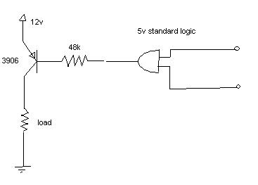
To turn the transistor off you will have to make the base and emitter voltages very similar, probably below 0.5V of each other. Since the emitter is tied to 12V you would have to make the base almost 12V too and that's impossible when you are driving it from 5V logic.
The trick to making it work is to place a resistor between the base and emitter so they assume a close potential and keep the transistor turned off. Then a second resistor goes from the base to the logic output. You select the values so when the logic is high, the base voltage is less than 0.5V lower than the emitter and when the logic is low, it is more than 0.6V lower than the emitter. The transistor will conduct when the logic output is low.
There are better ways of achieving this but the suggestion above uses the least number of components. You might run into problems if you are trying run the transistor in saturation, depending on the drive capability of the logic gate.
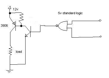
Yes, your new schematic is correct. the logic gate should be able to withstand the voltage, the resistor in it's output should be as high a value as possible though to give it as much protection as possible. The 2N3906 is only a small signal transistor so the base current only needs to be very low.
A far better way of doing this is to keep the resistor you added between the base and emitter, instead of connecting the other resistor to the logic gate, connect it to the collector of an NPN transistor. The emitter of that transistor goes to ground and the base is fed from the logic gate through another resistor. Sorry but I am unable to draw a schematic for you at the moment. It means two extra components, the NPN transistor and its new base resistor but it does make all the voltages fall within safe limits. It will however, invert the signal so you might need to change your logic functions slightly.
in last drwaing u have problem u drive the the base emiter of first transistore
without any resistore and first transistore driver second transistore without any
rb resistore i prefere to use that circuit
hi, I was wondering, using an active current source (PNP) on the SDA and SCL lines, where do I connect the base of the transistor? I believe the Collector is connected to the lines and the emitter is connected to the 3.3V source
This site uses cookies to help personalise content, tailor your experience and to keep you logged in if you register.
By continuing to use this site, you are consenting to our use of cookies.