grittinjames
Advanced Member level 1
- Joined
- Jun 1, 2006
- Messages
- 479
- Helped
- 44
- Reputation
- 90
- Reaction score
- 32
- Trophy points
- 1,308
- Location
- bangalore india
- Activity points
- 3,985
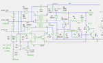
constant off-time smps
any how this is working very well for me. and i am using for all my battery charger and LED lighning purpose
any how this is working very well for me. and i am using for all my battery charger and LED lighning purpose
") ]
]