Continue to Site

Welcome to EDAboard.com

Welcome to our site! EDAboard.com is an international Electronics Discussion Forum focused on EDA software, circuits, schematics, books, theory, papers, asic, pld, 8051, DSP, Network, RF, Analog Design, PCB, Service Manuals... and a whole lot more! To participate you need to register. Registration is free. Click here to register now.

Which digital design is better ?

I came to know new things by reading and contributing to this topic

  • Yes

    Votes: 0 0.0%
  • No

    Votes: 0 0.0%
  • This topic is useless !

    Votes: 0 0.0%

  • Total voters
    0
Status
Not open for further replies.

vsmGuy

Advanced Member level 2
Joined
Jun 26, 2006
Messages
503
Helped
44
Reputation
88
Reaction score
15
Trophy points
1,298
Location
VddVss
Activity points
3,882
Hi !

I have made two sets of logically equivalent designs, one on each row, i.e, the gate hook up in the bottom is logically equivalent to the gate hookup just above it..

For example, the one on first row, first column is logically same as that in second row, first column, or , the one on first row, third column is logically same as that in second row, third column.

3_1205430546.gif


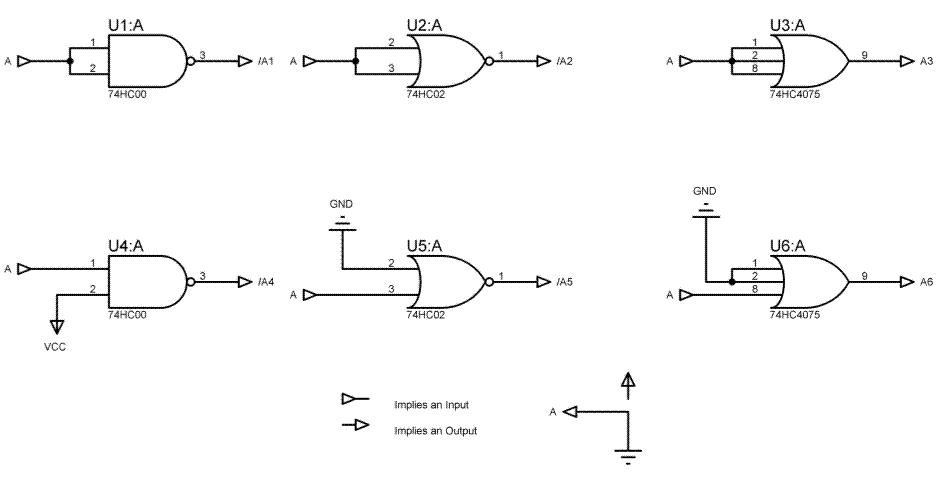
Given an option, which design you would choose over the other (i.e the top one or the bottom one) and why ?

The why is the most important.

If anyone is going to highlight terms like nonuniform propagation delay, he better show something in print, like quote a datasheet or DSO outputs.

If you find this topic insightful, please vote too !
 

Anecdotes, design suggestions, guidelines, tips welcome !
 

I am afraid it is impossible to see the image clearly. It is very small and the magnification doesn't work.

Added after 11 minutes:

Well, I have downloaded it and now it is clear.
It looks like the results will be very close. You have to know the inside structure of gates to decide which one to choose.
I would prefer the most left decisions, because the NOR has more complicated structure than NAND. And it is better to use a gate with smaller count of pins.
Anyway, it is only my opinion.
 

    vsmGuy

    Points: 2
    Helpful Answer Positive Rating
Assume they are normal, over the counter, 74HC components at ~5V with appropriate decoupling.
 

Come on have a look.. specially people with real designs under their belt !!

Jot down your thoughts !

Where are the advices on glitches ? Current consumption ? Noise susceptibility ?

Are these questions simple ? That's why no one answers them ?
 

vsmGuy said:
Come on have a look.. specially people with real designs under their belt !!

Jot down your thoughts !

Where are the advices on glitches ? Current consumption ? Noise susceptibility ?

Are these questions simple ? That's why no one answers them ?

Do not belive this forum is the holy grail.
Most of the questions are you asking here (noise, current consumption, glitches) can't be guessed from a simple logic drawing, telling nothing about the technology used for gates.
Things are simple. One gate input is better than two or three in parallel. One unused gate input to ground is better than one unused gate to VDD. And so on, nothing too special in your question.
 

    vsmGuy

    Points: 2
    Helpful Answer Positive Rating
melc said:
One unused gate input to ground is better than one unused gate to VDD.

What about (N)AND Gates where you cannot ground an input ?

What would you do then ?

Short both inputs or hook one to Vcc ?

melc said:
Things are simple. One gate input is better than two or three in parallel.

My point exactly !

Jot down your thoughts !

I told that consider them as run of the mill 74HC parts ! I have even the part numbers written beside them !

What would you do if you had these options while making a digital design using exclusively these parts ?

I know the question I have asked in this thread is nothing special.. but something tells me, people who have designed digital designs using such ICs hava whole lot to tell on this very simple issue..

I would like to hear from them !
 

I am afraid you last quation is not clear enough (at least for me).
Anyway, to connect an input of a (N)AND gate to ground is a serious mistake (you will not damage it but it will not work at all).
The better is to connect it to Vcc by a resistor (it will not load the driving output and the circuit will work faster).
If you use (N)OR you must connect the unused inputs to the Ground (through a resistor - pull-down).
 

    vsmGuy

    Points: 2
    Helpful Answer Positive Rating
dmk said:
I am afraid you last quation is not clear enough (at least for me).

No problems... which question ?

dmk said:
Anyway, to connect an input of a (N)AND gate to ground is a serious mistake (you will not damage it but it will not work at all).

Of course. You are effectively "disabling the gate".. That's exactly what I said before..

melc shared with us that it's better to ground inputs, and I put forward the situation where that would not work.

There is an idea that power planes are susceptible to noise and not ground planes.

I would love to see a few references stating this idea !

dmk said:
The better is to connect it to Vcc by a resistor (it will not load the driving output and the circuit will work faster).

Could you tell me "it will not load the driving output" a little more clearly ?

I would love to see a few references stating this idea !

dmk said:
If you use (N)OR you must connect the unused inputs to the Ground (through a resistor - pull-down).

Why not directly connect to ground instead of a pull down ?

Would I be crazy if I said that would in fact introduce the possibility of noise creeping in ?
 

Hi,
Unless I am left with only any one of the other options, I would prefer circuit U5:A , because,

1. It has only unit loading on the input.

2. Disabling the second input by connecting it to ground for an OR gate is better than using a two input Nand with an input connected directly to Vcc. When Vcc connection is not current limitted by a resistor, the gate input capacitor can sometimes blow up the input due to initial surge current.

3. Minimum cell configuration from the given choices so that you can get more gates in a given package.

4. I prefer not to vote because I feel that you got more out of me than me from your post.!!!

Regards,
Laktronics
 

    vsmGuy

    Points: 2
    Helpful Answer Positive Rating
vsmGuy said:
melc said:
One unused gate input to ground is better than one unused gate to VDD.

What about (N)AND Gates where you cannot ground an input ?

What would you do then ?

Short both inputs or hook one to Vcc ?

Read this first:
https://focus.ti.com/lit/an/scla007a/scla007a.pdf
Shorting two inputs means double parasitic capacitance. If you need to transfer a clk at the gate transfer frequency limit, then you don't connect two inputs together.
If you have some HC logic connected to your PIC, than you can connect it in the easiest way for routing, PIC is lazy


melc said:
Things are simple. One gate input is better than two or three in parallel.

My point exactly !

Jot down your thoughts !

I told that consider them as run of the mill 74HC parts ! I have even the part numbers written beside them !

Didn't noticed untill you pointed.

What would you do if you had these options while making a digital design using exclusively these parts ?

I know the question I have asked in this thread is nothing special.. but something tells me, people who have designed digital designs using such ICs hava whole lot to tell on this very simple issue..

I would like to hear from them !
 

    vsmGuy

    Points: 2
    Helpful Answer Positive Rating
"There is an idea that power planes are susceptible to noise and not ground planes."
They both are susceptible to noise (that is why you can often see "power rails"). Sometimes it's possible that not the whole current flows through the Vcc (if you have more than one supply voltages - say +5V, 3.3V, +-12, etc.). But it will always flow through the ground. That's the reason the ground is more important than the power supply.
"Could you tell me "it will not load the driving output" a little more clearly ?"
Each output has sa called "fanout" - the (maximum) number of inputs it can drive. So, first it's good not to load the output if there is no need. Second, each input (as well as the wire, connected to it) has a parasitic (stray) capacity. Each time the output change its state, it must charge or discharge it. In most cases it is not important (in low freqs). Any way, the output must insure different current for 1 or 2 inputs it has to drive. Sometimes this causes troubles.
"Would I be crazy if I said that would in fact introduce the possibility of noise creeping in ?"
No, you are not crazy saying this. It is correct. Nevertheless it is better (not obligatory) to use pull-up/down resistors (just to prevent the damage of inputs when the device is power on).
 

laktronics said:
Unless I am left with only any one of the other options, I would prefer circuit U5:A

Thanks for answering !

Actually my question was, if you had to choose between :

1. U1A and U4A

2. U2A and U5A

3. U3A and U6A

Which of 1, 2 and 3 would you choose ?

The choice is not the thing I am looking for, the reasoning is !

laktronics said:
3. Minimum cell configuration from the given choices so that you can get more gates in a given package.

Could you try and clarify more ?

For example, melc has done an excellent job of giving a very good reference that will be useful to anyone in this field.

Many new entrants in this field still don't know it was TI that fabricated the first Si Transistor, and that is how they became a nondescript company from Texas to a giant they are now.

laktronics said:
4. I prefer not to vote because I feel that you got more out of me than me from your post.!!!

Ha ha !

Actually, I kept the poll more for the readers of the thread than the people who already know the answers.

I created this thread so that we will have experienced designers commenting on basics and errors that beginners do, so that they understand what these errors are and do not commit it.

The poll is for such beginners who I hope will come to know more about such "simple" issues as this one and become better designers by knowing the basics well.

That is why I need help from experienced designers to comment on this.

I am sure the information we will see revealed on this thread will assert that there are a lot of things to think about before we apply simple boolean algebra while designing our circuits.

Believe me - I have seen many designs where CMOS pins are floating, pins directly connected to power, decoupling capacitors far away from the ground pins of the IC they decouple.

This should not go on. If we have these issues at one place, people will understand flaws in their designs and of others and take care.

After all, why would anyone want to make bad circuits when they know better designs ?

I think you understand the reason why I created this thread.

Help me build it.

Added after 13 minutes:

dmk said:
"There is an idea that power planes are susceptible to noise and not ground planes."

They both are susceptible to noise (that is why you can often see "power rails"). Sometimes it's possible that not the whole current flows through the Vcc (if you have more than one supply voltages - say +5V, 3.3V, +-12, etc.). But it will always flow through the ground. That's the reason the ground is more important than the power supply.

Excellent point !

Thanks for taking my hint (and the bit of sarcasm in the statement) !

I don't know why the other contributors did not notice this line.

Both rails are susceptible to noise, and infact ground is the one with utmost importance. I understand that in this time of ASICs a design using 74xx is crazy, but basics are important.

I have seen questions on ground bounce etc all over this board, and they don't make sense to answer unless you have a few scenarios.

So I created this.

dmk said:
"Could you tell me "it will not load the driving output" a little more clearly ?"
Each output has sa called "fanout" - the (maximum) number of inputs it can drive. So, first it's good not to load the output if there is no need. Second, each input (as well as the wire, connected to it) has a parasitic (stray) capacity. Each time the output change its state, it must charge or discharge it. In most cases it is not important (in low freqs). Any way, the output must insure different current for 1 or 2 inputs it has to drive. Sometimes this causes troubles.

Yes, this reasoning you have given is ok for very general case.

But in HC family, one HC O/P is designed to drive approx 40 - 50 I/P.

I would love to stand corrected :)

dmk said:
"Would I be crazy if I said that would in fact introduce the possibility of noise creeping in ?"

No, you are not crazy saying this. It is correct. Nevertheless it is better (not obligatory) to use pull-up/down resistors (just to prevent the damage of inputs when the device is power on).

A quick note.

The suggestion of a resistor in series with the pin might have the same schematic of a pull up/down resistor but they are there for different reason.

The term I was searching for is "current limiting resistor" which is conceptually different from the function of a pull up/down resistor which defines the state of an I/P when no external signal is acting on the I/P in reality.

There is another reason to have a pull up/down resistor besides defining the default state of the I/P.

Any guess ? The answer lurks in this thread itself !

:)

As usual, any statement I have made in this reply - I would love to stand corrected :)
 

Yes, the HC common fanout is 40, but it has a load capacitance, too.
Yes, there is a difference in pull-up and pull-downd resistors, probably it was better to say pulled down (up) resistor.
A direct connection to the 5V (power supply) is not recommended, since an input transient of over 5.5V can damage some TTL devices, ones that use a multi-emitter transistor in the input stage. The pull-up resistor limits current and prevents damage in this case.
 

dmk said:
"There is an idea that power planes are susceptible to noise and not ground planes."
They both are susceptible to noise (that is why you can often see "power rails"). Sometimes it's possible that not the whole current flows through the Vcc (if you have more than one supply voltages - say +5V, 3.3V, +-12, etc.). But it will always flow through the ground. That's the reason the ground is more important than the power supply.


A good designed ground plane will allways have lower impedance than a V+ supply (anyone will be that one), just because the V+ ( or V-) comes from a power supply with miliohms output impedance in the best situation, while the ground plane will be allways the reference.
You can't say that "ground is more important than power supply". Both are important as well, that's why has been invented the ZBC technology where the isolation between ground and power plane is 1mil (ZBC1000) or 2mil (ZBC2000) creating distributed filtering capacitors.
**broken link removed**
 

Thanks melc, I agree. But in most cases (not so speedy designs, etc.) you always cares much more about the ground (plane), than the power supply.
 

In fact, the return path matters, not the ground or power supply.
 

As per your assumptions I, as I am sure others reading this have designed many boards where the above situation required a decision. After consulting various manufacturers data sheets I found that most of them suggest that connecting directly to the power rail is fine. I usually connect both inputs together purely because it often simplifies PCB design. If this is not practical and you must tie it to the supply then using a pull up / pull down does give you the assurance that only a limited amount of current could flow through the input at any given time, power up, static discharge etc. When using a resistor there is the bonus benefit that it is still fairly easy to use the gate when you discover only after PCB manufacture that you require an extra logic element to get your circuit to work correctly:D
 

I would have loved to see more people find this topic useful .. anyways time will tell.

I have found most of the replies to the topic insightful.. I will consider my attempt moderately successful.

It will be even better if more people contribute to the thought process..

But Ii would like to stress that one should always consider the initial transient state of the digital circuit.

That is something we let go easily.

If time permits, I will show you all a circuit where due to parasitic loading of the NOT gate I/P, the circuit was in oscillation.

I also cannot stress enough to use current limiting resistors for direct connections to ground or power.

Stabilized power even from a SMPS or LM7085 have an intial setup time mentioned in the DS.

The I/P resistor hack described above is another way of popularizing the practise of limiting resistors... they can be used for later patch jobs.

Plus, always keep at mind the slew rate of the gates.. they are kept under an assumption for loading.

The logical design can follow boolean algebra, but circuit design should strictly follow appropriate design rules.

Digital circuits are not outside the effects of the analog world.
 

Status
Not open for further replies.

Part and Inventory Search

Welcome to EDABoard.com

Sponsor

Back
Top