Continue to Site

Welcome to EDAboard.com

Welcome to our site! EDAboard.com is an international Electronics Discussion Forum focused on EDA software, circuits, schematics, books, theory, papers, asic, pld, 8051, DSP, Network, RF, Analog Design, PCB, Service Manuals... and a whole lot more! To participate you need to register. Registration is free. Click here to register now.

segment display board interfacing with PIC Micro

Status
Not open for further replies.

Djsarkar

Member level 3
Joined
Jul 27, 2020
Messages
55
Helped
0
Reputation
0
Reaction score
1
Trophy points
8
Activity points
301
Hi

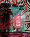
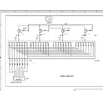
I want to display single digit up counter. I have PIC18F45K80. I am using MPLABX 5.40 and XC8 2.30.
The picture below shows a typical seven-segment display board. Seven segment displays are of two types: common anode and common cathode

a) Is this common cathode type display ? I think yes
b) How to select first Display ?
 

Attachments

  • 7 segment.jpg
    7 segment.jpg
    54.1 KB · Views: 115

Yes, common cathode

Take CN1 pin 1 high to select digit 1

Keep CN1 pins 2,3,4 low

Put a high on each pin a b c d e f g and DEC for each segment that you want lit
 
Hi,

The schematic is not according standards. But it's not wrong, either.

Better way is to draw the most positive supply on top, the most negative supply on bottom of the sheet.
Then the current flow is from top to bottom.
Signal (information) should be left to right.
The use of GND and supply symbols makes the schematic more easy to read.

Klaus

Btw: use interrupt for automatic display update with fixed timing.
And read how others did it ... also to avoid "ghosting"
 
@KlausST

The schematic is clipped from manufacturers schematic - OP has no control of it (except to re-draw from scratch)

And yes - the bigger schematic is terrible (but better than nothing - just)

The schematic is not according standards
It attempts to reach "abysmally poor" standard (but fails to meet it)
 
Hi,

I agree.
I didn'want to say the OP did something wrong.
So everthing is fine :)

Klaus
 

Yes, common cathode

Take CN1 pin 1 high to select digit 1

Keep CN1 pins 2,3,4 low

Put a high on each pin a b c d e f g and DEC for each segment that you want lit

Can you tell me when I select all four display , why only three of them are working. Why all four not working together

S1 = S2 =S3 =S4 = high
Is it the problem of power? I am using 12v DC/1A DC
**broken link removed**
 

Attachments

  • IMG_20201002_185952.jpg
    IMG_20201002_185952.jpg
    2.2 MB · Views: 95

Hardware issue - floating (unconnected) pins are of unknown level

Why only one jumper wire - why not 4 ??

Looks like you connected low to digit 1 and left the other three digits unconnected.

Post all code, not just a single line
 
Last edited:
Hardware issue - floating (unconnected) pins are of unknown level

Why only one jumper wire - why not 4 ??

Looks like you connected low to digit 1 and left the other three digits unconnected.

Post all code, not just a single line

connections

S1-- RB0
S2-- RB1
S3-- RB2
S4-- RB3

A--D0
B--D1
C--D2
D--D3
E--D4
F--D5
G--D6
DEC-D7

Program

C:
#define _XTAL_FREQ 8000000
#include <xc.h>
// PIC18F45K80 Configuration Bit Settings
// 'C' source line config statements
// CONFIG1L
#pragma config RETEN = OFF      // VREG Sleep Enable bit (Ultra low-power regulator is Disabled (Controlled by REGSLP bit))
#pragma config INTOSCSEL = HIGH // LF-INTOSC Low-power Enable bit (LF-INTOSC in High-power mode during Sleep)
#pragma config SOSCSEL = HIGH   // SOSC Power Selection and mode Configuration bits (High Power SOSC circuit selected)
#pragma config XINST = OFF       // Extended Instruction Set (Enabled)
// CONFIG1H
#pragma config FOSC = INTIO2    // Oscillator (Internal RC oscillator)
#pragma config PLLCFG = OFF     // PLL x4 Enable bit (Disabled)
#pragma config FCMEN = OFF      // Fail-Safe Clock Monitor (Disabled)
#pragma config IESO = OFF       // Internal External Oscillator Switch Over Mode (Disabled)
// CONFIG2L
#pragma config PWRTEN = OFF     // Power Up Timer (Disabled)
#pragma config BOREN = SBORDIS  // Brown Out Detect (Enabled in hardware, SBOREN disabled)
#pragma config BORV = 3         // Brown-out Reset Voltage bits (1.8V)
#pragma config BORPWR = ZPBORMV // BORMV Power level (ZPBORMV instead of BORMV is selected)
// CONFIG2H
#pragma config WDTEN = OFF      // Watchdog Timer (WDT disabled in hardware; SWDTEN bit disabled)
#pragma config WDTPS = 1048576  // Watchdog Postscaler (1:1048576)
// CONFIG3H
#pragma config CANMX = PORTB    // ECAN Mux bit (ECAN TX and RX pins are located on RB2 and RB3, respectively)
#pragma config MSSPMSK = MSK7   // MSSP address masking (7 Bit address masking mode)
#pragma config MCLRE = ON       // Master Clear Enable (MCLR Enabled, RE3 Disabled)
// CONFIG4L
#pragma config STVREN = ON      // Stack Overflow Reset (Enabled)
#pragma config BBSIZ = BB2K     // Boot Block Size (2K word Boot Block size)
// CONFIG5L
#pragma config CP0 = OFF        // Code Protect 00800-01FFF (Disabled)
#pragma config CP1 = OFF        // Code Protect 02000-03FFF (Disabled)
#pragma config CP2 = OFF        // Code Protect 04000-05FFF (Disabled)
#pragma config CP3 = OFF        // Code Protect 06000-07FFF (Disabled)
// CONFIG5H
#pragma config CPB = OFF        // Code Protect Boot (Disabled)
#pragma config CPD = OFF        // Data EE Read Protect (Disabled)
// CONFIG6L
#pragma config WRT0 = OFF       // Table Write Protect 00800-01FFF (Disabled)
#pragma config WRT1 = OFF       // Table Write Protect 02000-03FFF (Disabled)
#pragma config WRT2 = OFF       // Table Write Protect 04000-05FFF (Disabled)
#pragma config WRT3 = OFF       // Table Write Protect 06000-07FFF (Disabled)
// CONFIG6H
#pragma config WRTC = OFF       // Config. Write Protect (Disabled)
#pragma config WRTB = OFF       // Table Write Protect Boot (Disabled)
#pragma config WRTD = OFF       // Data EE Write Protect (Disabled)
// CONFIG7L
#pragma config EBTR0 = OFF      // Table Read Protect 00800-01FFF (Disabled)
#pragma config EBTR1 = OFF      // Table Read Protect 02000-03FFF (Disabled)
#pragma config EBTR2 = OFF      // Table Read Protect 04000-05FFF (Disabled)
#pragma config EBTR3 = OFF      // Table Read Protect 06000-07FFF (Disabled)
// CONFIG7H
#pragma config EBTRB = OFF      // Table Read Protect Boot (Disabled)

#define S1            LATBbits.LATB0
#define S2            LATBbits.LATB1
#define S3            LATBbits.LATB2
#define S4            LATBbits.LATB3

#define SevenSegment         LATD

void Port_pins_Initialized (void);

void main(void)
{
  Port_pins_Initialized ();

         LATBbits.LATB0 = 1;
         LATBbits.LATB1 = 1;
         LATBbits.LATB2 = 1;
         LATBbits.LATB3 = 1;
    while (1)
    {

       
         SevenSegment = 0x00;
         __delay_ms(1000);
       
          SevenSegment = 0x01;
         __delay_ms(1000);
       
           SevenSegment = 0x02;
         __delay_ms(1000);
       
           SevenSegment = 0x03;
         __delay_ms(1000);
       
             SevenSegment = 0x04;
         __delay_ms(1000);
       
       
    }
   
}

void Port_pins_Initialized (void)
{
    LATA = LATB = LATC = LATD = LATE =  0;

    TRISA = 0b0000000;// all are output, Unused
    TRISB = 0b0000001;// B0 connected to switch button
    TRISC = 0b0000000;// LED to C2
    TRISD = 0b0000000;//  All are output, Unused
    TRISE = 0b0000000;// All are output, Unused

    ANCON0 = 0; // digital port
    ANCON1 = 0; // digital port
    CM1CON = 0; // Comparator off
    CM2CON = 0; // Comparator off
    ADCON0 = 0; // A/D conversion Disabled
}


segment.jpg
 

I don't think there's a problem with the code. I think it's a hardware issue. I have a connected only Four pins of PORTB and The remaining four pins not connected anywhere. should I connect these pins to ground?
 

"I don't think there's a problem with the code." I think that there is - I see an obvious mistake
" I think it's a hardware issue." I see no reason to think that

Rather than spoon-feed you with the answer - I will leave you to learn how to solve your own problems.

Comment every single line of your code. Make it very clear what what function every line is supposed to perform

Any mistakes may become obvious to you once you add remaining comments.

Uncommented code is bad code :(

... and NO ... never short outputs to ground
 
Last edited:

Rather than spoon-feed you with the answer - I will leave you to learn how to solve your own problems.
Thanks Hexreader for quick reply Your answer makes me think that after writing better code, the problem can be solved. Ok i'll come back with code
 

Rather than spoon-feed you with the answer - I will leave you to learn how to solve your own problems.
I have solved problem myself. In my first code problem that I was making pin RB0 as input by mistake

Program display number from 0, 1, 2, 3 on segment board continuously

C:
#define _XTAL_FREQ 8000000
#include <xc.h>
// PIC18F45K80 Configuration Bit Settings
// 'C' source line config statements
// CONFIG1L
#pragma config RETEN = OFF      // VREG Sleep Enable bit (Ultra low-power regulator is Disabled (Controlled by REGSLP bit))
#pragma config INTOSCSEL = HIGH // LF-INTOSC Low-power Enable bit (LF-INTOSC in High-power mode during Sleep)
#pragma config SOSCSEL = HIGH   // SOSC Power Selection and mode Configuration bits (High Power SOSC circuit selected)
#pragma config XINST = OFF       // Extended Instruction Set (Enabled)
// CONFIG1H
#pragma config FOSC = INTIO2    // Oscillator (Internal RC oscillator)
#pragma config PLLCFG = OFF     // PLL x4 Enable bit (Disabled)
#pragma config FCMEN = OFF      // Fail-Safe Clock Monitor (Disabled)
#pragma config IESO = OFF       // Internal External Oscillator Switch Over Mode (Disabled)
// CONFIG2L
#pragma config PWRTEN = OFF     // Power Up Timer (Disabled)
#pragma config BOREN = SBORDIS  // Brown Out Detect (Enabled in hardware, SBOREN disabled)
#pragma config BORV = 3         // Brown-out Reset Voltage bits (1.8V)
#pragma config BORPWR = ZPBORMV // BORMV Power level (ZPBORMV instead of BORMV is selected)
// CONFIG2H
#pragma config WDTEN = OFF      // Watchdog Timer (WDT disabled in hardware; SWDTEN bit disabled)
#pragma config WDTPS = 1048576  // Watchdog Postscaler (1:1048576)
// CONFIG3H
#pragma config CANMX = PORTB    // ECAN Mux bit (ECAN TX and RX pins are located on RB2 and RB3, respectively)
#pragma config MSSPMSK = MSK7   // MSSP address masking (7 Bit address masking mode)
#pragma config MCLRE = ON       // Master Clear Enable (MCLR Enabled, RE3 Disabled)
// CONFIG4L
#pragma config STVREN = ON      // Stack Overflow Reset (Enabled)
#pragma config BBSIZ = BB2K     // Boot Block Size (2K word Boot Block size)
// CONFIG5L
#pragma config CP0 = OFF        // Code Protect 00800-01FFF (Disabled)
#pragma config CP1 = OFF        // Code Protect 02000-03FFF (Disabled)
#pragma config CP2 = OFF        // Code Protect 04000-05FFF (Disabled)
#pragma config CP3 = OFF        // Code Protect 06000-07FFF (Disabled)
// CONFIG5H
#pragma config CPB = OFF        // Code Protect Boot (Disabled)
#pragma config CPD = OFF        // Data EE Read Protect (Disabled)
// CONFIG6L
#pragma config WRT0 = OFF       // Table Write Protect 00800-01FFF (Disabled)
#pragma config WRT1 = OFF       // Table Write Protect 02000-03FFF (Disabled)
#pragma config WRT2 = OFF       // Table Write Protect 04000-05FFF (Disabled)
#pragma config WRT3 = OFF       // Table Write Protect 06000-07FFF (Disabled)
// CONFIG6H
#pragma config WRTC = OFF       // Config. Write Protect (Disabled)
#pragma config WRTB = OFF       // Table Write Protect Boot (Disabled)
#pragma config WRTD = OFF       // Data EE Write Protect (Disabled)
// CONFIG7L
#pragma config EBTR0 = OFF      // Table Read Protect 00800-01FFF (Disabled)
#pragma config EBTR1 = OFF      // Table Read Protect 02000-03FFF (Disabled)
#pragma config EBTR2 = OFF      // Table Read Protect 04000-05FFF (Disabled)
#pragma config EBTR3 = OFF      // Table Read Protect 06000-07FFF (Disabled)
// CONFIG7H
#pragma config EBTRB = OFF      // Table Read Protect Boot (Disabled)

#define S1            LATBbits.LATB0
#define S2            LATBbits.LATB1
#define S3            LATBbits.LATB2
#define S4            LATBbits.LATB3

void Port_pins_Initialized (void); //prototype function

void main(void)  // main program start
{
   Port_pins_Initialized (); //// Initialize the device
  
    S1 = 1;    S2 = 1;     S3 = 1;    S4 = 1; // select all
    
    while(1)  //Run forever
    {
        S1 = 1; S2=S3=S4 =0; // select only  1st segment
        LATD = 0x3F;         // Display 0
        __delay_ms(1000);    // Wait 1 seconds
        
        S2 = 1; S1=S3=S4 =0; // select only  2st segment
        LATD = 0x06;          // Display 1
        __delay_ms(1000);     // Wait 1 seconds
        
        S3 = 1; S1=S2=S4 =0; // select only  3rd segment
        LATD = 0x5B;         // Display 2
        __delay_ms(1000);    // Wait 1 seconds
        
        S4 = 1; S1=S2=S3 =0;  // select only  4th segment
        LATD = 0x4F;           // Display 3
        __delay_ms(1000);// Wait 1 seconds
      }
    
    return ;
}

// Initialize the device
void Port_pins_Initialized (void)
{
    LATA = LATB = LATC = LATD = LATE =  0; // set all to 0

    TRISA = 0b0000000;// all are output, Unused
    TRISB = 0b0000000;// control signal S1, S2, S3, S4 (0-3))
    TRISC = 0b0000000;// All are output, Unused
    TRISD = 0b0000000;//  segment board connected 
    TRISE = 0b0000000;// All are output, Unused

    ANCON0 = 0; // digital port
    ANCON1 = 0; // digital port
    CM1CON = 0; // Comparator off
    CM2CON = 0; // Comparator off
    ADCON0 = 0; // A/D conversion Disabled
}
 
Status
Not open for further replies.

Similar threads

Part and Inventory Search

Welcome to EDABoard.com

Sponsor

Back
Top