Continue to Site

Welcome to EDAboard.com

Welcome to our site! EDAboard.com is an international Electronics Discussion Forum focused on EDA software, circuits, schematics, books, theory, papers, asic, pld, 8051, DSP, Network, RF, Analog Design, PCB, Service Manuals... and a whole lot more! To participate you need to register. Registration is free. Click here to register now.

How do I connect top layer with bottom layer on a MCU board?

Status
Not open for further replies.

Garyl

Full Member level 5
Joined
Mar 28, 2017
Messages
253
Helped
6
Reputation
12
Reaction score
7
Trophy points
18
Activity points
2,633
Dear all,
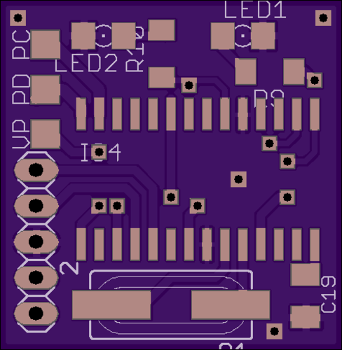
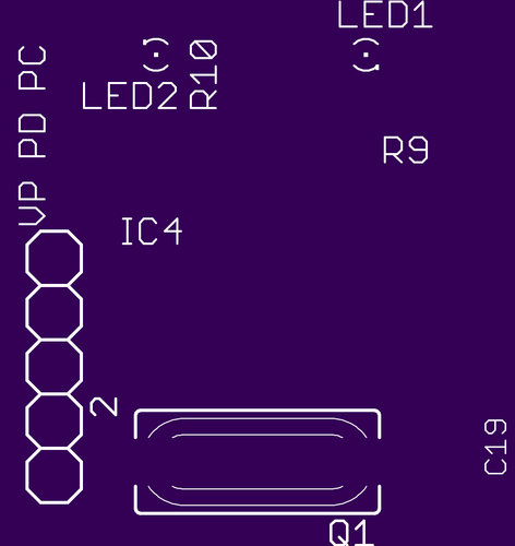
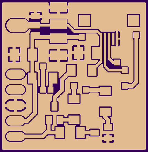
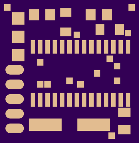
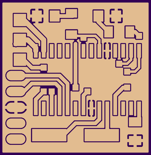
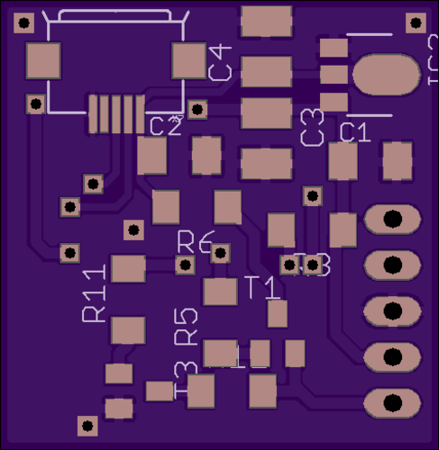
my PCB designed in eagle has top layer ground and bottom layer ground.
They both flood around other signal
How do I connect those ground coppers?
- single via at the center of the board?
- for each corner of board one via (4 * 1 = 4 vias)
- something else?
 

I think no. of vias required depends on current rating that is how much max current flows in that path. You can't place very big vias and so you have to increase no. of vias.
 

This is a microcontrollres forum and I asked in a relation to MCU board, there will be very little currents, I am more worried about the interference etc. it is a board with PIC18LF2550.
I heard that badly placed tracks can cause extra inductances and troubles
 

How many board layers? What is the highest signal frequency of the board?
Generally it is fine to place a number of smaller vias along the outer edges of the PCB to connect GND pours from top/bottom if they are there for purposes of reducing emissions or for allowing balance of current back to the power supply, especially if you have devices on top and bottom that are connecting to the GND pours. Where you may cause trouble is if you make alot of current have to travel across the PCB to follow lowest impedance path to get to the power supply return or earth ground. For example, if my PCB is tied to earth at one end of the PCB and the bottom side pour is connected to it, but the top side pour is only connected to the bottom side pour (and through that to the earth) through a couple vias at the oppositve end of the PCB, I am forcing return current from the top side devices to pass the entire length of the PCB, to reach the vias to reach the bottom side pour, and then traverse the length of the PCB again to get to the earth/ground connection point. This is an extreme example, but one to illustrate how that could be bad.
 

of course just two layers, top and bottom. PIC18LF2550 runs at maximum 20MHz.
 

of course just two layers, top and bottom

You might have already heard that the "ideal" ground would be a continuous plane allover the board, as it's usually implemented in multilayer PCB. On a two-layer board, you'll try at least to achieve a meshed ground, using so many vias as required to jumper the voids on one side by ground traces or pours on the other side (case three: something else).

This might work out on a not too densely populated board.

PIC18LF2550 runs at maximum 20MHz.
I guess, you can probably control radio interferences generated by the processor (if anybody cares about it at all), but have difficulties to achieve sufficient immunity against electrostatic discharges and nearby contact arcing with your two layer design.
 
  • Like
Reactions: Garyl

    Garyl

    Points: 2
    Helpful Answer Positive Rating
Hi,

I agree with FvM. Try to create a solid GND plane on one layer.
I´m not the friend of copper pour. And copper pour on both sides (like you described) is way worse than one solid GND plan and the othe without GND.

But for a detailed answer we should see your PCB layout.
And we need some more information about currents and frequencies.

Klaus
 
  • Like
Reactions: Garyl

    Garyl

    Points: 2
    Helpful Answer Positive Rating
I can show layout soon,
but now can you tell me, is using a "top layer for VDD" and "bottom layer for GND" better?

- - - Updated - - -

I can show layout soon,
but now can you tell me, is using a "top layer for VDD" and "bottom layer for GND" better?
 

The recommendations for creating dedicated layers for power and ground are very sound and are the result of many decades in the fabrication of such boards.
One advantage concerns your basic stripline/transmission line model - the circuit trace(s) with a fixed/constant dielectric and distance above a sold reference plane will have a consistent impedance.
For your simple board this isn't as critical as on a GHz ARM A9 with DDR3 RAM array, but it will still provide great advantage/improvement to how your PCB signals behave.
Having internal power & ground planes provide these consistent references planes for maintaining the trace impedances pretty well.
Without them, your trace impedance will vary by considerable amount and by whatever other copper they happen to be near, and what is on the other PCB side (which is also far away).
Additionally, the internal power and ground planes can be quite close together (e.g. 9 mils) and they form a relatively "tight" coupling which helps to improve our power supply rail regulation across the PCB, and reduce noise.

About the only PCBs that I design that are only 2 layer are purely analog ones - though even a number of them can benefit from dedicated power and ground plane layers.

Not everything HAS to have these layers, but it is very common for any circuit board with a micro to use them in the past ~25 years or so, unless one is making a very crude, inexpensive toy where a few pennies make a difference and functionality isn't that critical.

Show us your basic layout and we can offer more specific advice to help.
 
  • Like
Reactions: Garyl

    Garyl

    Points: 2
    Helpful Answer Positive Rating
Hi,

Yes, more layers have it's benefits.
But I designed a lot 2 layer PCBs.

You have to decide.
For low frequency to medium frequency applications one could use just two layers.
With two layer boards I try to generate a very solid GND at solder side, all signals including power is on the component side.
But all IC power connections are properly decoupled with capacitors to GND with very short wires..

...
There are many possible solutions..

Let's see your PCB.

Klaus
 
  • Like
Reactions: Garyl

    Garyl

    Points: 2
    Helpful Answer Positive Rating
Okay, so here is the current version of my PCB.
Please note:
- this is two layer PCB
- top and bottom layers are flooded with ground plane
- there are 3 vias connecting top ground and bottom ground
- there is a PIC18F on the board with crystal
- there is a 3.3V LDO on the board


Do You think that I can already order that board from manufacturer or should I redesign it?
I've worked on it for some time already and I can't make it smaller
Thanks in advance!
 

Hi,

Two layers...with both sides assembled..

It's difficult to achieve all the requirements regarding decoupling, EMI, EMC, ESD....

I could not verify the circuit, because I'm not familiar with PICs.
Afaik you need capacitors at the xtal.
Maybe there are other issues.

If you want somebody to verify your circuit you should provide the schematic.

Klaus
 

There should be a few more ground vias. You might e.g. improve the return path from Vcc bypass capacitors C3 + C1 to processor Vss pins. I agree about apparently missing crystal capacitors.

Without detailed information about the connected external circuit and application environment, it's hard to determine if the circuit has sufficient EM compatibility. If I understand the circuit correctly, the only external connection (besides ICSP connector for development/initial programming) is an USB jack.
 

Status
Not open for further replies.

Similar threads

Part and Inventory Search

Welcome to EDABoard.com

Sponsor

Back
Top