Continue to Site

Welcome to EDAboard.com

Welcome to our site! EDAboard.com is an international Electronics Discussion Forum focused on EDA software, circuits, schematics, books, theory, papers, asic, pld, 8051, DSP, Network, RF, Analog Design, PCB, Service Manuals... and a whole lot more! To participate you need to register. Registration is free. Click here to register now.

cascode amplifier and miller effect

Status
Not open for further replies.

arr_baobao

Full Member level 2
Joined
Nov 1, 2011
Messages
134
Helped
0
Reputation
0
Reaction score
0
Trophy points
1,296
Activity points
2,317
Hi guys,

how does the cascode amplifier in the pic below helps to solve the miller effect and improve the overall stability.
been reading about the miller effect, still don't quite understand it.
anyone can explained in the most simplest way?

cascode.JPG
 

The Miller Effect is due to the capacitance between the drain and gate.
This reduces the gate AC signal by coupling signal from the drain AC signal since the drain signal is 180 degrees out of phase with the gate (causing negative feedback).
If you reduce the drain AC voltage by using a cascode arrangement (which reduces the signal by the gain of the second transistor) then you also reduce the effect of the Miller Effect by the same factor.
 
The pic is not a cascode amplifier, it's one of a minimal comparator
(or an op amp, if you added frequency compensation and didn't
care about a lot of things).

The whole point of cascode is, your "steering" device which
has the transconductance-gain, is held at constant(-ish)
voltage so Miller effect (Cgd vs Rgg_sum) is negligible, and
the "guard" device takes the drain voltage swing but returns
the Cgd current to a stiff and not-in-the-gain-lineup point
where it doesn't steal or fight the signal.

But that structure is not illustrated here.

yes, this is 2 stage op amp. thanks for pointing out.
how does the op- amp works.
my understanding is the VINN(-ve) on the btm left nmos will always turn off the btm left nmos, and cause the both pmos to turn on.
then VINP(+ve) will turn on the btm right nmos and cause the voltage current flow to the right part of the pmos.
correct me if i'm wrong.

so my question now is, does this circuit has any miller compensation in it ?
if yes, how?

Why do you speak about "turn on" and "turn off"?
This is not a "digital" device but a linear amplifier, is it not?

Regarding "...current flow to the right part of the pmos"
Do you assume any current flowing into the gate of the MOS transistor?
 
In that circuit, which is not a cascode amplifier by the way, the output device still suffers from miller effect between gate and drain. Its not a good example.

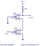
This is the classic cascode amplifier:
cascode.png

In this circuit the upper fet isolates the load resistor from the gate of the lower fet which does all the amplifying. There is now no direct (miller) capacitive coupling between the load resistor and the gate of the lower fet.

The lower fet can now have a lot of high frequency gain and a very wide bandwidth because the miller capacitance problem has been solved.
 
so my question now is, does this circuit has any miller compensation in it ?
if yes, how?

If there were Miller compensation it would appear as a
capacitor (or possibly drawn as a FET if using that type
of device as a capacitor) attached across the drain and
gate of the output PMOS. But obviously there is not.

Miller compensation attempts to turn to advantage, the
same effect that cascoding tries to kill. The added D-G
capacitance is locally multiplied in its effect by the transistor
gain. Sometimes so much so, that a "zero" element needs
to be added in series to prevent ruining HF response while
keeping the LF rolloff.
 

If there were Miller compensation it would appear as a
capacitor (or possibly drawn as a FET if using that type
of device as a capacitor) attached across the drain and
gate of the output PMOS. But obviously there is not.

lets say i added a cap across the D-G terminal in the circuit above for miller compensation purpose.
How the cap helps to mitigate the miller effect, what is the theory behind this.
And how do i decide/calculate the value for the cap.

thanks
 

The DG cap does not mitigate the miller effect, it utilizes it.

The purpose of miller compensation is pole splitting, creating a dominant low frequency pole and shifting the other pole to higher frequencies.

Compensation is dimensioned according to the intended open loop frequency characteristic, e.g. an unity-gain stable OP which allows stable operation with -1 feedback factor must have sufficient phase margin at |loop gain| = 1.
 
  • Like
Reactions: LvW

    LvW

    Points: 2
    Helpful Answer Positive Rating
The DG cap does not mitigate the miller effect, it utilizes it.

The purpose of miller compensation is pole splitting, creating a dominant low frequency pole and shifting the other pole to higher frequencies.

study through some online materials, regarding the miller compensation to improve stability.
why they spec it @ odB phase margin at least 45 degree.
why 0 dB gain ? and the relationship with the phase.
any material that can explain in "layman term"?

thanks
 

Well of course Teh InterWebz is full of information on frequency
compensation and stability.

The concern is that gain above unity, at a phase shift approaching
180 degrees, allows regenerative oscillation. 45 degrees is where
people feel they have some safety margin (although those who
have been down that road, may pick 60 degrees since there is
more to a real application than a schematic design and small
signal ideal response, and safer is better). The gain should have
gone to sub-unity well before the phase flips. You also look at
gain margin at the 180-phase point (because often there is a
cluster of overlapping poles and zeros near there, and monotonic
gain rolloff is not to be assumed).
 

Sometimes gain margin as well as phase margin is specified.
The gain margin is the gain (less than 1) at the point where the phase becomes 180°.
Normally you want the gain be much less than 1 at that point.
 

Hi guys,

how does the cascode amplifier in the pic below helps to solve the miller effect and improve the overall stability.
been reading about the miller effect, still don't quite understand it.
anyone can explained in the most simplest way?

View attachment 130735

This is a "cascade" (not cascode) of a diff amp and a CS amp; or a 2-stage opamp - and here we utilize (rather than "mitigate") Miller effect to improve the phase margin for making the amplifier stable when used in a negative f/b configuration.
If you search the web, you will get plenty of tutorials on Miller effect that causes the Cap between the G and D of the 2nd stage amplifier pmos to be multiplied and appear as a load at the o/p of the 1st stage, and hence producing a dominant pole at that node (much lower than the other pole at the 2nd stage o/p) - this is referred to as pole splitting.
Another way to explain is that for higher freq signals the Cap between the G and D of the 2nd stage amplifier pmos acts as short-circuit and passes the 1st stage o/p signal to the 2nd stage o/p without any appreciable phase shift, hence avoiding stability (low PM) problem.
 
This is a "cascade" (not cascode) of a diff amp and a CS amp; or a 2-stage opamp - and here we utilize (rather than "mitigate") Miller effect to improve the phase margin for making the amplifier stable when used in a negative f/b configuration.
.

thanks.

can i said that in cascode configuration, they are designed in that way to mitigate the miller effect.
whereas, in 2 stage op amp with negative feed back configuration, they utilize this miller effect to achieve a stable output at the op amp.
 

Put it this way.
Miller effect creates negative feedback which increases with frequency.
That is usually a very bad thing if you are trying to build a high frequency amplifier with sufficient gain at high frequencies.

There are circumstances where you WANT to build an amplifier where the gain rapidly reduces with frequency.
That is very commonly done to improve stability and reduce the chances of oscillation in high gain low frequency amplifiers.

In that case, its a desirable thing, and may even be increased further by fitting an actual physical "miller" capacitor to increase the effect.

So miller capacitance may be either good or bad, depending on what it is you are trying to achieve.
 

thanks.

can i said that in cascode configuration, they are designed in that way to mitigate the miller effect.
whereas, in 2 stage op amp with negative feed back configuration, they utilize this miller effect to achieve a stable output at the op amp.

Yes..you are right..in Cascode config. the placement of the CG stage (with low Rin) above the CS stage degrades the volt gain of the CS stage to ~1, so the Miller effect cap due to Cgd of CS amp is not much at the G, and thus, the pole made by this cap with the i/p source resistance (Rs, of i/p voltage source) will be at higher freq (yielding higher overall BW) than for a standalone CS amp.
[see
 

Status
Not open for further replies.

Similar threads

Part and Inventory Search

Welcome to EDABoard.com

Sponsor

Back
Top