Continue to Site

Welcome to EDAboard.com

Welcome to our site! EDAboard.com is an international Electronics Discussion Forum focused on EDA software, circuits, schematics, books, theory, papers, asic, pld, 8051, DSP, Network, RF, Analog Design, PCB, Service Manuals... and a whole lot more! To participate you need to register. Registration is free. Click here to register now.

Help need for obtaining EM Co-Simulation for 1GHz LNA design in ADS2011.10

Status
Not open for further replies.

narayani

Full Member level 2
Joined
Aug 15, 2014
Messages
120
Helped
0
Reputation
0
Reaction score
1
Trophy points
1,298
Activity points
2,262
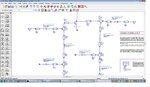
I have taken example of MW_Ckts > LNA_1GHz_wrk.7zap from the Agilent Advanced Design System 2011.10.

This is example for the layout design of 1 GHz Low Noise Amplifier ( LNA ). This 1GHz LNA, which contains both active( transistors), passive elements(R,L,C), and MLINS. From this schematic, we can generate the Layout of LNA.

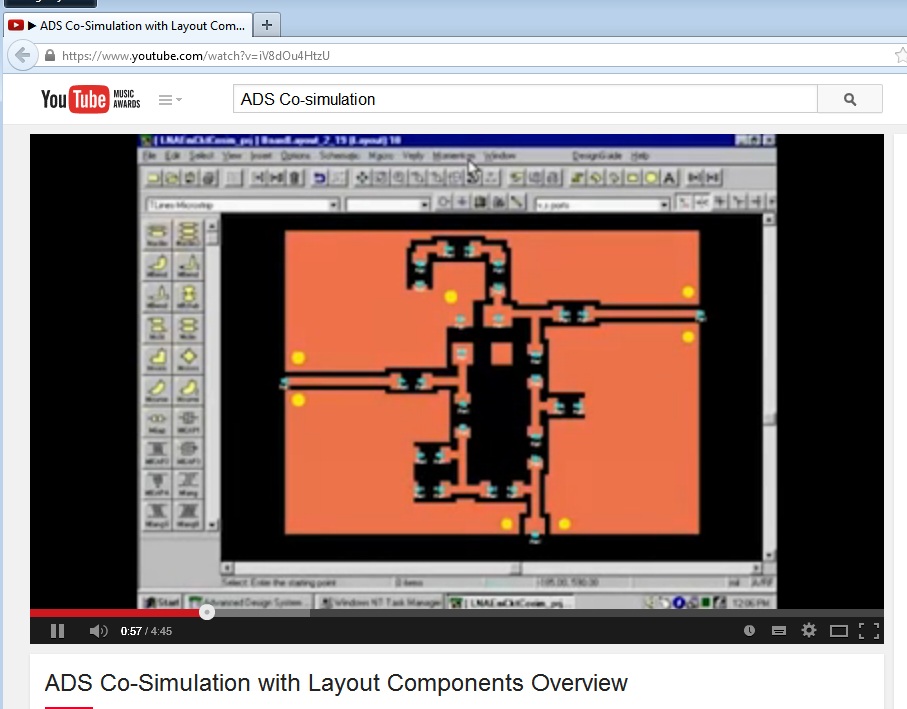
My question is, how to get the EM - Co Simulation for this 1GHz LNA schematic circuit. Can you anybody help me to get the EM -Co Simulation for this circuit.

Can you give guidelines, how to get the EM- Co-Simulation, when circuit is built for generating layout, which contains both passive and active elements.
 

Attachments

  • LNA_1GHz_Example.jpg
    LNA_1GHz_Example.jpg
    266 KB · Views: 125

First, you should create its layout with distributed elements in the schematic.Then you have to place the ports for lumped elements ( input and output ports,capacitors,resistors,transistors etc).After that you do a EM simulation carefully in Momentum ( pay attention for ports,meshing,frequency etc) and when EM simulation is succesfully terminated you should create a "layout look-like" view of your layout.Then you will able to place this view with appropriate ports in another schematic test-bench and connect other lumped elements to associated ports and finally do ypur simulations.
 
Thank you for your elaboration explanation. If somebody knows pdf help document of EM Co-Simulation for circuit contains both passive and active elements as I said in the posting #1. Can you show the help document.
 

It is exactly what BigBoss has mentioned.

But if you're using ADS 2014 or 2015, you'll find there is a "Co-Simulation" selection you can choose in which you don't need to add every port to lumped elements. It is very convenient.
 
First, you should create its layout with distributed elements in the schematic.

As you said, how to create its layout with distributed elements in the schematic as I have shown 1GHz LNA layout schematic generation circuit in the posting #1. In the posting # 1, I have shown the 1 GHz LNA Schematic layout generation circuit, from this schematic, we can generate the layout with all components (Transistors, R,L,C). How we can create the distribute elements for my circuit as shown in posting #1 and later we can place pins where ever the connections are existing. Can you help me to create distribution element for my circuit as shown in posting # 1.
Can you clarify it.
 

Already we have created LNA layout with Components. For EM Co-simulation, how we have to generate the LNA layout without components as shown below screen shots from the already existing LNA layout with components.


Status
Not open for further replies.

Part and Inventory Search

Welcome to EDABoard.com

Sponsor

Back
Top