milan.rajik
Banned
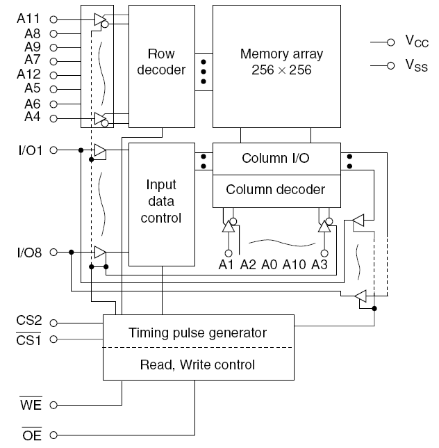
This is regarding to 8085 memory interfacing. In many books and other sources they mention that a RAM chip like 8K X 8 will have a CS pin connected to higher order address lines through address decoder circuit. A WR bar and RD bar lines which connect to Input tristate buffer and output tristate buffer. They also mention that there will be 8 input data lines to store data into RAM and 8 output data lines to read data from RAM but externally there will be only 8 bi-directional data bus. I want to know how the 8 input data lines and 8 output data lines are combined internally.