pusparaga
Full Member level 4
Dear Sir,
I want to use my design to Avago ATF54143 transistor. When I went through the datasheet of Avago ATF54143 transistor. I am getting the following doubts.
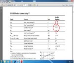
(1) He has given in the datasheet absolute maximum ratings as follows
Symbol Parameter Units Absolute Maximum
VDS Drain-Source Voltage V 5
VGS Gate-Source Voltage V -5 to 1
VGD Gate-Drain Voltage V -5 to 1
I DS Drain Current mA 120
From the above parameters, we can notice that Vgs, Vds, Vgd, Ids. He is saying in the datasheet Absolute maximum ratings of the above parameter. My doubt is , how to understand these values, whether we have to understand absolute values or potential difference values of Vgs,Vds, Vgd, Ids values.
What I understood about absolute value is , we have to take the difference of voltages with respect to the ground. Potential difference(Voltage Difference) is, we have to take differences of voltages, suppose VGS means Vg-Vs.
If anybody knows please clear above doubts. While designing, whether we have to take absolute voltages or difference of voltages.
If we take differences of voltages(Vgs), why he has given in the datasheet Absolute maximum ratings.
I want to use my design to Avago ATF54143 transistor. When I went through the datasheet of Avago ATF54143 transistor. I am getting the following doubts.
(1) He has given in the datasheet absolute maximum ratings as follows
Symbol Parameter Units Absolute Maximum
VDS Drain-Source Voltage V 5
VGS Gate-Source Voltage V -5 to 1
VGD Gate-Drain Voltage V -5 to 1
I DS Drain Current mA 120
From the above parameters, we can notice that Vgs, Vds, Vgd, Ids. He is saying in the datasheet Absolute maximum ratings of the above parameter. My doubt is , how to understand these values, whether we have to understand absolute values or potential difference values of Vgs,Vds, Vgd, Ids values.
What I understood about absolute value is , we have to take the difference of voltages with respect to the ground. Potential difference(Voltage Difference) is, we have to take differences of voltages, suppose VGS means Vg-Vs.
If anybody knows please clear above doubts. While designing, whether we have to take absolute voltages or difference of voltages.
If we take differences of voltages(Vgs), why he has given in the datasheet Absolute maximum ratings.