Continue to Site

Welcome to EDAboard.com

Welcome to our site! EDAboard.com is an international Electronics Discussion Forum focused on EDA software, circuits, schematics, books, theory, papers, asic, pld, 8051, DSP, Network, RF, Analog Design, PCB, Service Manuals... and a whole lot more! To participate you need to register. Registration is free. Click here to register now.

Low forward drop half wave rectifier

Status
Not open for further replies.

manishanand14

Full Member level 4
Joined
Sep 3, 2011
Messages
203
Helped
10
Reputation
20
Reaction score
9
Trophy points
1,308
Location
Bangalore ,India
Activity points
2,572
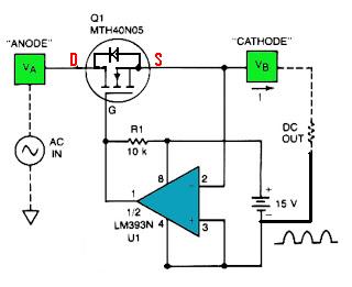
I came across this circuit

Low drop ut power supply.jpg
**broken link removed**

I am not able to understand how the current flow will happen from Source to Drain in an n- channel MOSFET. Also the body diode will conduct in the other half cycle.So how the circuit will work as explained in the article.
 

I think this circuit is wrong.
Drain current Id will flow in the opposite direction if the FET is placed in that way.

The drain always has to be at a higher potential than the source.

Here is my suggestion about the correction in the circuit.

6122891900_1389358792.jpg
 

I agree, but surely a MOSFET with a built-in diode will make it useless as a rectifier, the diode will always conduct in the reverse direction anyway.

Brian
 

Start with the first case where Va is more positive than Vb and the MOSFET is turned off. The Q1, source-drain diode starts to conduct. This puts a negative voltage on the U1 inverting input relative to the non-inverting input which is at the same voltage as Va. The output of U1 then goes as far positive as possible (let us say about +13 volts) in relation to Va. This puts a large, positive gate-to-source voltage on the MOSFET which turns it on. The trick is the MOSFET is now operating in the "Triode" mode where the channel acts like a resistor. Current can flow in either direction. The MOSFET channel now takes over the conduction and current no longer flows through the source-drain diode. The "rectifier" is now conducting.

The next case is where Va goes more negative than Vb. The Q1, source-drain diode does not conduct and the U1 inverting input will be positive in relative to the non-inverting input. The U1 output is near the voltage at Va and the gate-to-source voltage is below the threshold of Q1. The "rectifier" is now off.

Here are a couple of concerns. First, the drain-source breakdown voltage of the MTH40N05 is 50 volts. Do not expect this circuit to handle line voltages of 120VAC or higher. Select a MOSFET appropriate for the AC voltage to be rectified. Second, the LM393 common mode voltage range is the negative supply. This circuit requires the inverting input to go a little below the negative supply voltage. This is probably OK but the input is operating out of the specified input range by a small amount. Third, it is not predictable what the voltage on the U1 inverting input will be when Q1 turns off. Is it positive enough to keep the U1 output at the negative power rail? Some leakage will probably do the trick.

Some additions - Leakage of Q1 when off may be enough to get the U1 output to go high and turn on Q1. It may not be necessary for the source-drain diode to conduct. Also, it would be good to add some input protection on the U1 inverting input. When Q1 is conducting, it may be possible to exceed the negative input range of the device. A series resistor and clamp diode may be a good addition.
 
Last edited:
The trick is the MOSFET is now operating in the "Triode" mode where the channel acts like a resistor. Current can flow in either direction.

Please clarify this.

You mean bidirectional current flow will happen through a MOSFET in Ohmic or Linear region.

- - - Updated - - -
 
Last edited:

Yes, it is my understanding that when Vgs >> Vds, the channel acts like a resistor and current can go either way. The graphs of Vds and drain current for different Vgs end at the 0,0 origin but the physics does not magically end there.
 

The original circuit has a serious limitation in the AC voltage which can be rectified. The peak AC voltage must be less than the DC power to the op amp. Otherwise, when the MOSFET is off, the peak voltage across the MOSFET is greater than the allowable voltage on the inverting input of the op amp. Adding a series resistor and clamping, Schottky diodes protects the inverting input and allows large AC voltages. It also deals with my concern with input voltage less then the negative supply. The picture shows an updated version of the circuit and simulation result.
 
Analog Ground is correct about the bidirectional current flow. The internal diode is the only thing preventing a MOSFET being used as a bi-directional switch.

The internal diode isn't even strictly necessary. There's a PN junction between the source-drain channel and the substrate, and power MOSFET designers are in the habit of connecting the substrate to the source, so you effectively end up with a diode between source and drain.

Apparently there are some small signal MOSFETs that have a fourth pin for the substrate, instead of connecting it to the source. Those would be more versatile.

btw, JFETs don't have that diode and they are sometimes used in the triode region as variable resistors for AC signals e.g. for gain control. You're likely to find that sort of thing e.g. in Dolby noise-reduction circuitry.

A lot of JFETs are actually completely symetrical so it doesn't matter if you swap the drain and source connectios even in a linear amplifier with the JFET operating in saturation.

- - - Updated - - -

Happy coincidence - I've just seen an advert on the front page of the forum for a low-drop bridge rectifier solution that works on the same principle as your circuit. See here: https://www.linear.com/product/LT4320?utm_source=LT4320&utm_medium=bnr&utm_campaign=EDABoard
 
The internal diode isn't even strictly necessary. There's a PN junction between the source-drain channel and the substrate, and power MOSFET designers are in the habit of connecting the substrate to the source, so you effectively end up with a diode between source and drain.
You are right that source-substrate connection isn't required by MOSFET operation principle, nevertheless it's effectively unavoidable in power MOSFET design, a bit more than a habbit.

The capability of inverse conduction is obvious both from elementary device equations as well as MOSFET datasheets. And it's used in a large number of circuits, e.g. synchronous buck converters and MOSFET H-bridges. You just didn't notice it if you are confused about the circuit in post #1.
 
You are right that source-substrate connection isn't required by MOSFET operation principle, nevertheless it's effectively unavoidable in power MOSFET design, a bit more than a habbit.
Oh, oops! pity.
 

Drawback: If you put a filter capacitor on output as required in most cases, it will be another story. It will always be conducting. A separate rectified half wave signal using a diode and supplied to IC input can be a solution then.
 

Drawback: If you put a filter capacitor on output as required in most cases, it will be another story. It will always be conducting.
Are you referring to the circuit in post #1? Then the analysis is incorrect. The circuit will work as a synchronous rectifier, at least theoretically. In practice, deriving the control signal from the Vds polarity won't work so well considering comparator offsets. Also the requirement of a floating supply doesn't suggest it as a real circuit solution. Other restrictions have been mentioned by Analog Ground.
 

My bad, I overlooked supply connections. I once used this function to drop 0.6V (trickle charge state) in a 3.6V lithium battery charger when charging voltage reached 4.3V.
 

Status
Not open for further replies.

Similar threads

Part and Inventory Search

Welcome to EDABoard.com

Sponsor

Back
Top