Continue to Site

Welcome to EDAboard.com

Welcome to our site! EDAboard.com is an international Electronics Discussion Forum focused on EDA software, circuits, schematics, books, theory, papers, asic, pld, 8051, DSP, Network, RF, Analog Design, PCB, Service Manuals... and a whole lot more! To participate you need to register. Registration is free. Click here to register now.

Calculated inductive stub on FET source L=..., connect halves L/2 , or both pins L?

Status
Not open for further replies.

Terminator3

Advanced Member level 3
Joined
Feb 25, 2012
Messages
802
Helped
71
Reputation
142
Reaction score
63
Trophy points
1,308
Activity points
9,027
Hello! After calculating inductive stub, i have problem how to attach it in microstrip: FET have two source pins.
Assume my inductive stub is L, how i must attach it?
1) attach L short stub to one of source pins, other source pin is directly grounded
or
2) attach L to both of source pins.
3) maybe attach L/2 to both source pins?
 

First variant is for sure wrong. You can either use your second variant if the inductance is maybe large enough or use variant 3. But with 3) you have maybe problems with symmetry. But this dependence on frequency and layout. I would prefer variant 2).
 
Thank you!
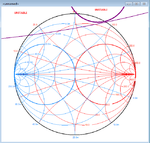
I also have question regarding oscillations. At 6GHz stability circles are:
stabilitycircles.png
In current case both circles are stable outside. For oscillator, we start from putting some network reflect coefficient in instable area (currentrly inside circles).
In my opinion both instable areas are small, and i see problem here. But is there really a problem here? I just think, that it would be difficult to match such oscillator, because stable area is small.

S11=PolarToRect(0.814,-64.8)
S11 = 3.465843433e-1 - 7.365292207e-1i
S12=PolarToRect(0.053,46.1)
S12 = 3.67502969e-2 + 3.818920892e-2i
S21=PolarToRect(4.130,104.3)
S21 = -1.020105923e0 + 4.002034971e0i
S22=PolarToRect(0.482,-48.8)
S22 = 3.174883198e-1 - 3.626639861e-1i

delta=S11*S22-S12*S21
delta = 3.324760289e-2 - 4.676520194e-1i

k=(1-Abs(S11)^2-Abs(S22)^2+Abs(delta)^2) / (2*Abs(S12*S21))
k = 7.42116621e-1

stability factor 0.7 seems ok for oscillator. I tried to add inductance to source pin and alter S parameters, but k factor becomed ever bigger, and i want smaller..
 

Maybe can you post your schematic?
 

Here what i do:
schinfo.png
I do calculations in SpeqMath, stability circles drawn in Smith v3.10 (Prof.Fritz)

So actually it is preliminary phase:
after calculating stability factor and looking at circles, i see that instable regions are all in upper part of Smith chart.
I am not sure if there any way i can bring them down.

S parameters -> i convert them to Z matrix -> add inductive stub to source -> convert Z matrix back to S parameters
calculating k factor gives even bigger k factor.
 

So as I understood you want to build a oscillator based only on a unstable transistor? Why you don't use standard oscillator types, e.g. collpits or hartly?
 

What the S-Parameter indicate for different Microstrip circuits. What must me there MAX and/or MIN value for good performance of system.
 

johnjoe
So as I understood you want to build a oscillator based only on a unstable transistor? Why you don't use standard oscillator types, e.g. collpits or hartly?
Because i want to use microstrip ring resonator

microwave79
What the S-Parameter indicate for different Microstrip circuits. What must me there MAX and/or MIN value for good performance of system.
i just learn this. For good oscillator performance k<1, for amplifier k>1. So values near 1 is not very good. Amplifier can oscillate, oscillator do not start. If S11 or S22 far from 50 Ohm (smith cart center), need to match. You can take free program to draw stability circles and see is it difficult to build good matching for certain purpose. Most rf transistors already can oscillate at some frequency without matching and digging into S parameters =)
 
Last edited:

Designing an oscillator based on the instability of the transistor is totally wrong.
Actually an oscillator should be based on a stable amplifier (and a feedback network) with well defined open loop gain and phase influence at working frequency.
Otherwise this gives an oscillation that will be strong affected by many factors, as temperature, transistor bias, transistor parasitics, external passive components, etc.

Find the book "Discrete Oscillator Design" of R. Rhea (one of the best book ever for oscillator design) and you will be surprised to see there all the example oscillators are presented as open loop amplifiers.
 

Designing an oscillator based on the instability of the transistor is totally wrong.
Miscrostrip series feedback oscillator is this case? Can series feedback be made using approach from that book? I am not sure i want to buy it, i already bought two books on microwave design.
 

Hello again!
it is still unclear to me, in simulation there is only one source pin. In reality i have two source pins.
Phase on S11 differs from simulation if i attach microstrip to both source pins. I want to make simulation be more realistic.
So i still have this question:
After calculating inductive stub, i have problem how to attach it in microstrip: FET have two source pins.
Assume my inductive stub is L, how i must attach it?
1) attach L short stub to one of source pins, other source pin is directly grounded
or
2) attach L to both of source pins.
3) maybe attach L/2 to both source pins?
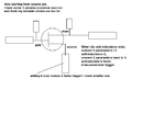
what i must do in simulation and what in reality to make results look better. Otherwise simulation is useless!
When i cut source pin result looks more realistic +-10deg, but i do not like it can damage FET somehow.
thanks =)
 

Presumed the source stub design makes sense, we would assume two parallel stubs of 2*L replacing a single L stub, isn't it?
 

Status
Not open for further replies.

Part and Inventory Search

Welcome to EDABoard.com

Sponsor

Back
Top