Continue to Site

Welcome to EDAboard.com

Welcome to our site! EDAboard.com is an international Electronics Discussion Forum focused on EDA software, circuits, schematics, books, theory, papers, asic, pld, 8051, DSP, Network, RF, Analog Design, PCB, Service Manuals... and a whole lot more! To participate you need to register. Registration is free. Click here to register now.

How to design a boost converter

Status
Not open for further replies.
A

ankushl

Guest
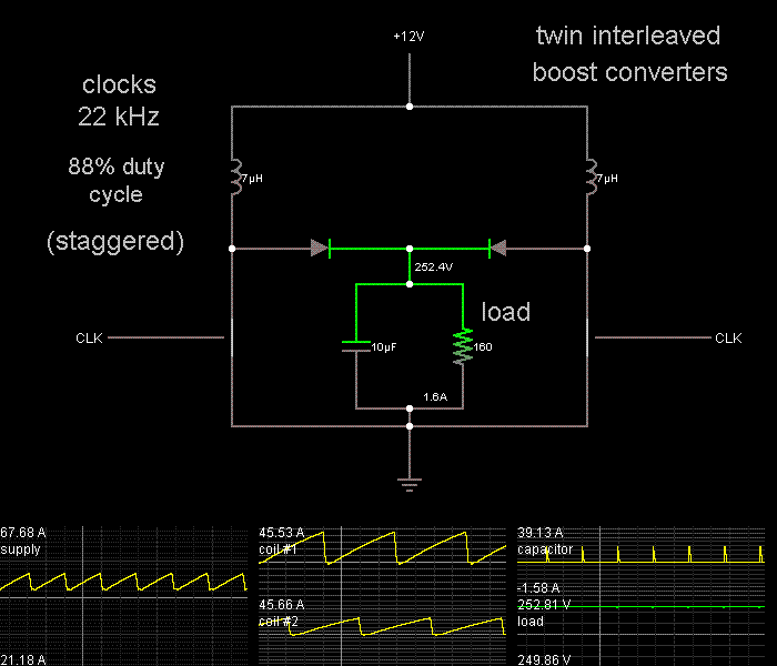
Hello...i am attempting to design a boost converter for the first time...what i need to do is boost the voltage from 12VDC to 240VDC with 1.5A...is this possible? or do i need to have an input dc voltage of at least 24VDC. I referred to the circuit from Rashid's Power Electronics Handbook...in the book, instead of a mosfet that i have used, is a simple spst switch with a diode value of D=0.5. I used a load value of 160 ohms. I am not able to understand how to choose the value of the diode and the switch parameters...the remaining component values i used as default from the text book. I understand that I have to use the equations to determine the values of components to be used. Also, the above circuit is for a PWM boost converter, I do not need PWM and the circuit is supposed to be for continuous conduction mode operation...I am a newbie, so please bear with me...is there any other circuit i could use? Please help...thanks

boost.jpg
 

Attachments

  • boost.jpg
    boost.jpg
    60.3 KB · Views: 92

What is your input supply - battery or low voltage transformer? What is the rated current output of the 12V supply? The method of achieving a higher output voltage (boost) will be using Pulse Width Modulation.
 

    V

    Points: 2
    Helpful Answer Positive Rating
I do not know the current rating, I am using a battery whose default value is 12V DC. This PWM circuit (obtained from Power Electronics Handbook) was made in NI Multisim and I chose the default voltage source which is a battery. There is no option for entering a current rating, and I could not find any option for entering the current rating either.
 

If you want 240V at 1.5A then you must input 30A at 12V, or 15A at 24V. Add 15 percent to make up losses. You will need to make sure there is very little resistance, in order to pass 30A.

This is a jump of 20X. It may work better if you were to interleave two or more boost converters.

To get an idea whether your design is possible...

Click to view the thread below. I posted links to interactive animated simulations of buck, boost, and buckboost converters.

You can edit the values to match your schematic. Or first it might help to watch how the coil action is supposed to happen. The scope traces tell the story.

https://www.edaboard.com/threads/268178/
 

    V

    Points: 2
    Helpful Answer Positive Rating
Hi bradtherad...thank you for your help...i do not understand a couple of things though...

first what do you mean by interleaving? do you mean that i should try connecting two boost converters one after the other in series to achieve the desired result?

second, i am confused as to how to select the values of L and C. do i have to select a large value of L and C to get a larger boost voltage, or do just one of them have to be high, and the other low? if so which one?

nice work with the animations, i am still working through them, was busy with something else in the last few days :)

in the animation for the boost converter, i changed the CLK waveform type to 12VDC, however, there seems to be no boost taking place...same result with the an AC 60Hz waveform (did not change the phase and the DC offset)...when i tried the simulation with these settings, i got a yellow exclamation mark briefly, which i am assuming is some sort of warning...

i also wanted to know if there is some sort of boost converter IC i could use that would fit the requirements of the boost converter that i want to design...
 
Last edited:

1.

Interleaving refers to two or more converters operating in parallel. The control clocks are staggered.

Screenshot:


Notice that the large step-up ratio requires a long duty cycle. The output cycle causes the capacitor to be subjected to strong current spikes. You would probably need a bank of several capacitors in parallel, with a total value of 10uF or so.

2.

Or it is also possible to use a two-stage method as you mentioned.

Say, one converter stepping up 12V at 30A to 60 at 6A. Then the output goes to a second converter to reach 240V at 1.5A.

3.

Since there is a certain amount of wasted power with a boost converter (more so with this large a step-up ratio)...

you may want to consider using a transformer to step up the volt level. An H-bridge would turn DC into AC square waves.
 

    V

    Points: 2
    Helpful Answer Positive Rating
Large output:input voltage ratios can be difficult to achieve, especially if you want to operate at a high switching frequency. In general I recommend that you keep your minimum on/off time longer than 20x the rise/fall times of your SMPS. So if your tr/tf is 100ns, and you need a duty ratio of 0.95, then that means you should operate with a frequency of 25KHz or lower. Your output ripple current will be pretty high though...
 

    V

    Points: 2
    Helpful Answer Positive Rating
hi bradtherad...what im trying to do is develop an in-car system which will allow me to charge a mobile phone, laptop and run a PMDC fan (the fan will be run for atleast 8hrs) without burdening the vehicle's existing electrical system. Due to their low weight and small form factor, i'm thinking of using Li-Ion batteries. I have to still think of a method of charging the batteries.

Specifications of the laptop charger:
Input: 100-240V ~ 1.5A Operating freq is 50-60Hz. System is for an Indian vehicle. In India, input voltage at home is 230-240V.

Phone Charger specifications:
Input: 100-240V ~ 100mA, 50Hz.

Fan specifications: 12V DC, 6W, 10 inch, 1600 RPM, 3 speed

Since the phone and laptop can be charged with 60Hz wave only, how do i obtain the same results without a 22kHz wave (whose frequency does not meet either charger's specifications)? I understand the two clock sources are necessary for the two interleaved boost converters. But how do i decide by how much they should be staggered? Thanks for the circuit...

- - - Updated - - -

Hi mtwieg...i need the boost converter's output to be a 60Hz wave and i will be using a battery, not an SMPS...how do i reduce the output ripple current?
 

Hi bradtherad...i tried the circuit you gave in Labcenter Proteus as this software allowed me to give a clock input, unlike NI Multisim. However, I get the error 'real-time' simulation failed to start'. The circuit and both clock settings are attached in the following images:

boost.jpg

clk1.jpg

clk2.jpg

Not able to figure out what i'm doing wrong with the simulation and the circuit...also, there was no option to enter the current for the battery in Proteus
 

Status
Not open for further replies.

Similar threads

Part and Inventory Search

Welcome to EDABoard.com

Sponsor

Back
Top