Continue to Site

Welcome to EDAboard.com

Welcome to our site! EDAboard.com is an international Electronics Discussion Forum focused on EDA software, circuits, schematics, books, theory, papers, asic, pld, 8051, DSP, Network, RF, Analog Design, PCB, Service Manuals... and a whole lot more! To participate you need to register. Registration is free. Click here to register now.

11 Amp PCB trace narrows down to 1.5mm.....is this OK?

Status
Not open for further replies.
T

treez

Guest
Hello,

I have a 1 oz copper PCB, and there is a trace on it which is 2.5cm long and 3mm wide.

...this trace carrys 11 Amps (RMS) of current.

For a 1cm length of this, the trace width goes down to 1.5mm wide.


Is this going to be ok?

It won't mean the PCB trace overheating and getting warped?

....it just seems fantastical that 11 Amps can "squeeze" through a 1.5mm trace neck?
 

I have not done the calculation for you. But in general, the length is in the equation in how wide the trace need to be. It is the total resistance of the trace that dissipates the power. The longer the trace, the higher the resistance the trace is IF YOU KEEP THE WIDTH THE SAME. The higher the resistance, the more power the trace dissipates and more it get hot.

Case in point, I designed IC before, the traces inside the IC is in microns width, how can they carry a few amps? This is because they are short. It is not the absolute width that is important, it is the width to length ratio that is important.

To calculate with your example, if both are same thickness......1oz:
1) 2.5cm and 0.3cm width gives 25/3=8.333
2) 1cm and 1.5mm width gives 10/1.5=6.67

The 1cm and 1.5mm width is even better. Hope that helps.

An important note, all these are for DC current or low frequency stuff. If you talk RF, the thickness of copper don't matter as skin effect kicks in, it does not matter you use 1/4, 1/2 or 1oz copper. The current density does not penetrate that deep.
 
  • Like
Reactions: treez

    T

    Points: 2
    Helpful Answer Positive Rating
Thanks, its not RF but is 11 Amps with a waveshape which is a rectified 50KHz sine wave current waveform.....so its an 100KHz frequency..................so yes, i will still need to look into skin effect?
 

Yes, calculate the skin effect. But you do have a DC component as it is a "half" or double sine wave with a DC component. So you do have two things to worry. Keep it wide and thick!!!
 
  • Like
Reactions: treez

    T

    Points: 2
    Helpful Answer Positive Rating
I don't know much about the calculation. But if it is in bottom layer (or top layer with clearance around the track), you can remove the lacquer masking over the track & fill it with full of lead. If you can(or if you want), solder a copper with in top of the track. It may handle several ten's of amp current...

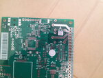
This is one of my design & it can handle up 25A current with lead filled....
20130102_134543.jpg
 

Skin depth at 100 kHz is about 0.2 mm. Skin effect won't be a problem in this situation. You get an increased current density at the trace edges.

The said 11A /1.5 mm trace is clearly above generally accepted PCB current density. Due to small dimensions, overheating should be tolerable, though.
 
  • Like
Reactions: treez

    T

    Points: 2
    Helpful Answer Positive Rating
look for Saturn PCB toolkit.
https://www.saturnpcb.com/pcb_toolkit.htm
Skin effect 100KHz 0.35um copper will be 100%.
I wouldn't reccomend using solder coating to increase current capacity as it is not easy to controll the thickness of the coating and solder has a greater resitivity than copper, safer to use the correct thickness copper, though it is done, Iamnot a fan of it for the previously mentioned reason. If you go for a UL registered product they will measure the temperature of the traces carrying high current...
There are though many different factors that can effect a traces ability to cary a said current, mainly down to how well the heat can be disipated, so if your trace connects to a thick connector pin some heat will be removed through that, but for these sort of calculations you realy require some serious software such as "comsol physics". Me I like to play safe and make shure I have enough copper, fusing is not my major concern, but causing a fire is.
 
  • Like
Reactions: treez

    T

    Points: 2
    Helpful Answer Positive Rating
I wouldn't reccomend using solder coating to increase current capacity as it is not easy to controll the thickness of the coating and solder has a greater resitivity than copper, safer to use the correct thickness copper, though it is done, Iamnot a fan of it for the previously mentioned reason. If you go for a UL registered product they will measure the temperature of the traces carrying high current...
I see solder "plumped up" traces with some cheap SMPS boards. Solder resistivity is about factor 8 higher than copper, so you need 1/4 mm solder cover to reduce 1 oz trace resistance by half. Not mind-blowing, but it's an option.
 

Hard to judge temperature rise without seeing the surrounding layout. If the trace is connected to large pours of copper at both end, or its directly on top of a large copper pour, then heating probably won't be an issue.
 

Yes its an option for cheeper cost concious designs, but not reccomended, very hard to quality control.
probably and WONT be an issue are the concerns here, I prefer to engineer designs so I know there WONT be an issue.
 

I can see a problem coating with lead, for AC, the skin effect force more current into the lead layer which is lower conductance and thereby generates more heat. It will help in the DC situation.

Skin effect \[\delta_c= \frac {1}{\sqrt{\pi \;f \;\mu \sigma}}=\frac {1}{\sqrt{3.14\times 100\times 10^3\times 2\times 3.14\times 10^{-7}\times 6\times 10^{7}}\], which is about 0.2mm. Double check my numbers. I guess skin effect is not that bad with copper.....BUT covering up with lead will easily pile over 0.2mm of lead and that is not nice!!!!
 

I woul dhave thought the greater the metal thickness , the lower the conductance at any frequency?
 

Not if the current density are all in the lead where it has lower conductance than copper.
 

Two ounce plus boards are available at very little extra cost, unless you are at the bottom line for costs I would use the required base thickness of copper to carry the current. i have never liked the practice of beefing up tracks with solder.
it would be tin/lead not lead and only if you have a lead free exception, otherwise it would be a lead free based solder, you cannot solder with lead alone. Again Quality controll of the coating thickness is hard to do and makes the assembly process harder to maintain, so you get no gains from using the correct copperin the first place.
 

The thing is that if you are passing HF current through a mix of lead and copper, the HF will flow more in the copper....................because as you say, its lower conductivity.....

...but some will still flow in the lead.and overall , the conductivity will be lower than if it were the copper bit alone.
 

Were getting at cross purposes here, I do not advocate using a solder coating on top of the copper full stop. What I am saying is use the correct wieght copper. I havn't personaly seen this done for many many years (going back to late 1980's when it was common, as well as the practice of HASL covering the whole of the copper pattern, under the solder resist.
 
  • Like
Reactions: treez

    T

    Points: 2
    Helpful Answer Positive Rating
I agree, I would not use solder on the trace just for that purpose. Does it cost more for heavier weight copper like 2 or 3 oz? But even it cost more, it would cost more to put solder onto the trace.......labor!!!!

In this case, the frequency is in between, it is not exactly a good example as it kind of work with solder!!!

If you have existing boards that you burn the trace, you have no choice, then yes put solder to beef up the trace will work for low frequency. It will not work for high frequency where skin effect come into play. You'll loss one surface to the lead with less conductance. But if you are laying out a new board, do it the right way.
 

Status
Not open for further replies.

Part and Inventory Search

Welcome to EDABoard.com

Sponsor

Back
Top