Continue to Site

Welcome to EDAboard.com

Welcome to our site! EDAboard.com is an international Electronics Discussion Forum focused on EDA software, circuits, schematics, books, theory, papers, asic, pld, 8051, DSP, Network, RF, Analog Design, PCB, Service Manuals... and a whole lot more! To participate you need to register. Registration is free. Click here to register now.

[SOLVED] Trouble passing LVS because of subc in IBM .18um technology

Status
Not open for further replies.

sonofflynn

Junior Member level 2
Joined
Mar 22, 2012
Messages
22
Helped
0
Reputation
0
Reaction score
0
Trophy points
1,281
Activity points
1,426
Hi,

I'm having trouble passing LVS in Calibre for an inverter I made using IBM .18um technology. My problem is due to the sub! pin in the layout. I've read several threads on the forum already discussing this issue, in particular, these two:


Here is a summary of what I have tried and what the results were:

1. If I delete the sub! pin from the layout, LVS runs but returns one error (missing port).

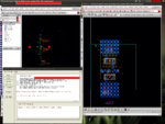
2. If I leave the sub! pin in the layout, and change the layer type to sxcut:label, LVS does not run and gives me the error, "Supply error detected. ABORT ON SUPPLY ERROR is specified - aborting". I've attached a screenshot of this as well.

Any help would be greatly appreciated.
 

Attachments

  • Screenshot at 2012-07-28 09:42:02.png
    Screenshot at 2012-07-28 09:42:02.png
    370.9 KB · Views: 301
Last edited by a moderator:

At the schematic focus on the subc component.The down-terminal of this device should have a net attached on it and respectively named as sub!
Start from this and LVS again!

Note : I recommend not to use globals for the supply rails (vdd! & gnd!).Choose another name like VDD,VSS/GND that is not already reserved.
 
Hi jimito13,

Thanks for the reply. I tested your suggestion..but it did not work. I still get the same error. Here is the screen shot.

Screenshot at 2012-07-28 18:26:57.png

Also, as you can see I changed gnd! to VSS, per your suggestion. I tried to change vdd! to VDD, but I got an error while creating the netlist before running LVS. Here is the screenshot for that problem.

Screenshot at 2012-07-28 18:22:39.png
 

Thanks for the reply. I tested your suggestion..but it did not work. I still get the same error. Here is the screen shot.

sxcut label sub! in your layout is not properly defined if i remember well...it should be defined with the drawing layer (drw/dg from LSW/palette) if i remember well.
You must study your pdk documentation to see what is the proper substrate methodology.This is confidential stuff i can't give more details i,have the documents
but i can't share them!The best you can do is to send a query to IBM if you can't proceed with this sub problems!

For the second issue i have no idea...maybe you didn't check and save your schematic before LVS...also an update components and nets at the layout side
is maybe necessary.

A final remark : you make use of devices with inherited connections,i am not pretty sure if subc is necessary in this case...try to substitute these devices with
those that have an extra pin for the bulk connection.In this case nmos sub node should be routed to sub! and pmos bulk node should go to VDD or vdd! depending
on the name you give for your positive rail.
 
I tried changing the sub! pin layer type from sxcut:ll to sxcut:dg, but still get the same error message, "Supply error detected. ABORT ON SUPPLY ERROR is specified - aborting".
 

What about this (my latter suggestion) :
A final remark : you make use of devices with inherited connections,i am not pretty sure if subc is necessary in this case...try to substitute these devices with
those that have an extra pin for the bulk connection.In this case nmos sub node should be routed to sub! and pmos bulk node should go to VDD or vdd! depending
on the name you give for your positive rail.

One question...have you tried with ASSURA instead of Calibre software?IBM from my experience recommends ASSURA for their PDK.Ignore this if your documentation recommends Calibre.
 

I did change the nwell connection on the pfet device from vdd! to VDD (my pin name). I have not tried ASSURA, however.

- - - Updated - - -

I finally fixed the problem... After selecting 'Generate --> All from source', I deleted the 'sub!' PIN that was created. I then created a 'sub!' LABEL, with the layer set to sxcut:label. LVS passed after this. Thanks for the help jimito13.
 

Status
Not open for further replies.

Part and Inventory Search

Welcome to EDABoard.com

Sponsor

Back
Top