Continue to Site

Welcome to EDAboard.com

Welcome to our site! EDAboard.com is an international Electronics Discussion Forum focused on EDA software, circuits, schematics, books, theory, papers, asic, pld, 8051, DSP, Network, RF, Analog Design, PCB, Service Manuals... and a whole lot more! To participate you need to register. Registration is free. Click here to register now.

Transmission gate D-flip flop simulation issue

Status
Not open for further replies.

viperpaki007

Full Member level 5
Joined
Jul 2, 2008
Messages
270
Helped
11
Reputation
22
Reaction score
8
Trophy points
1,298
Location
Finland
Activity points
3,395
Hi,

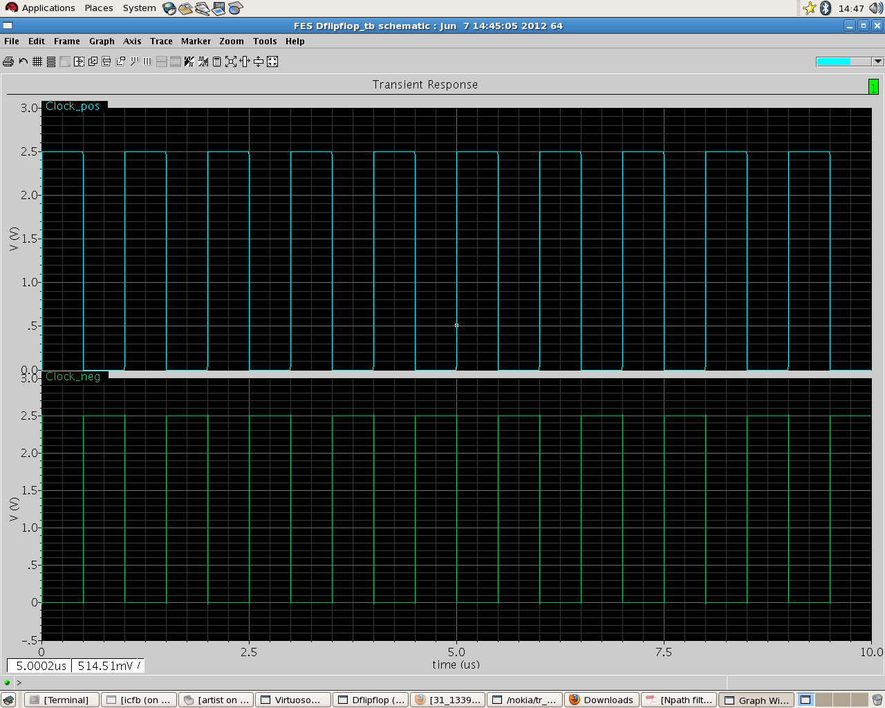
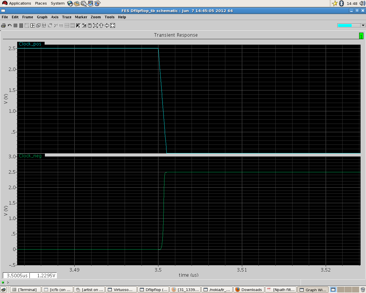
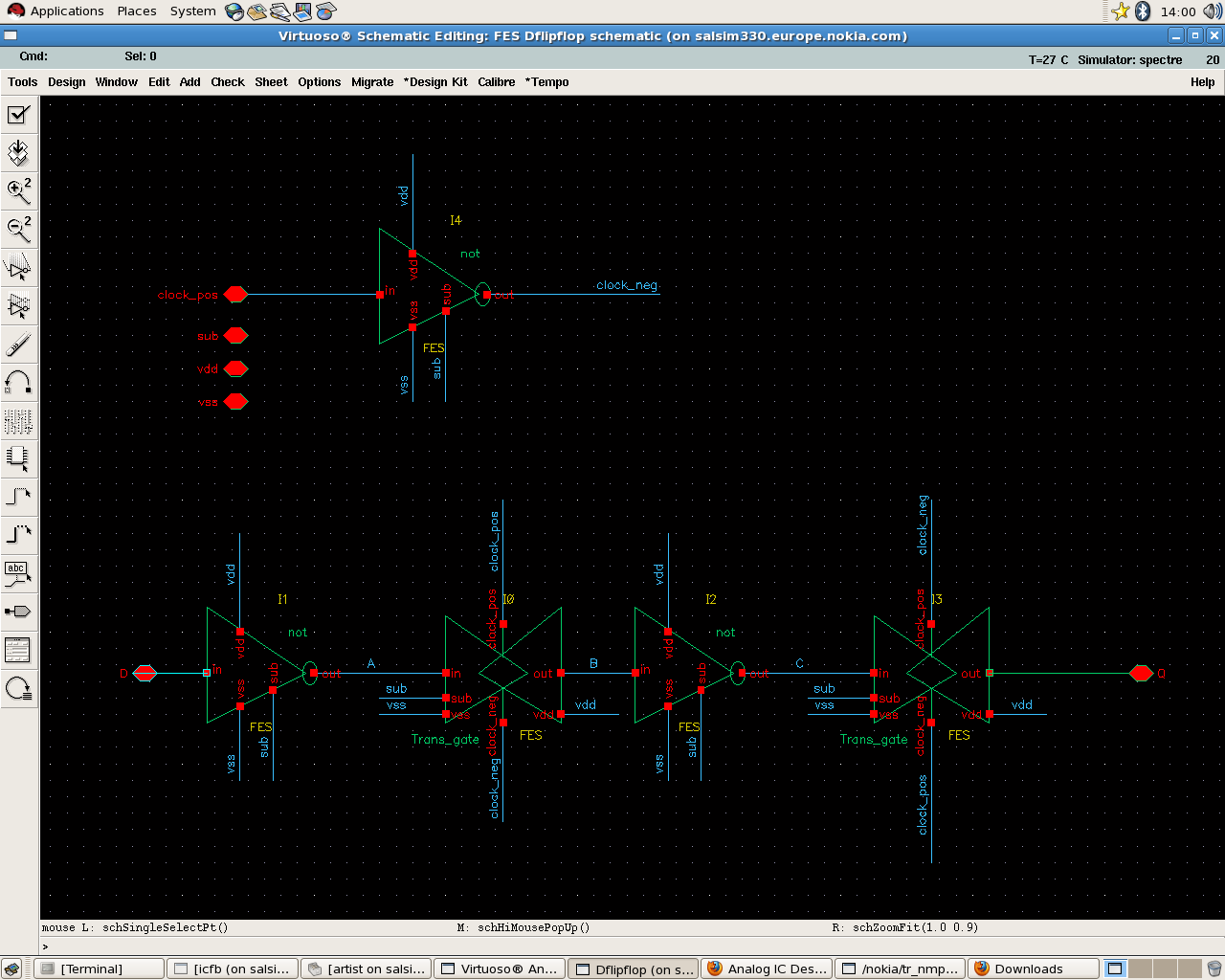
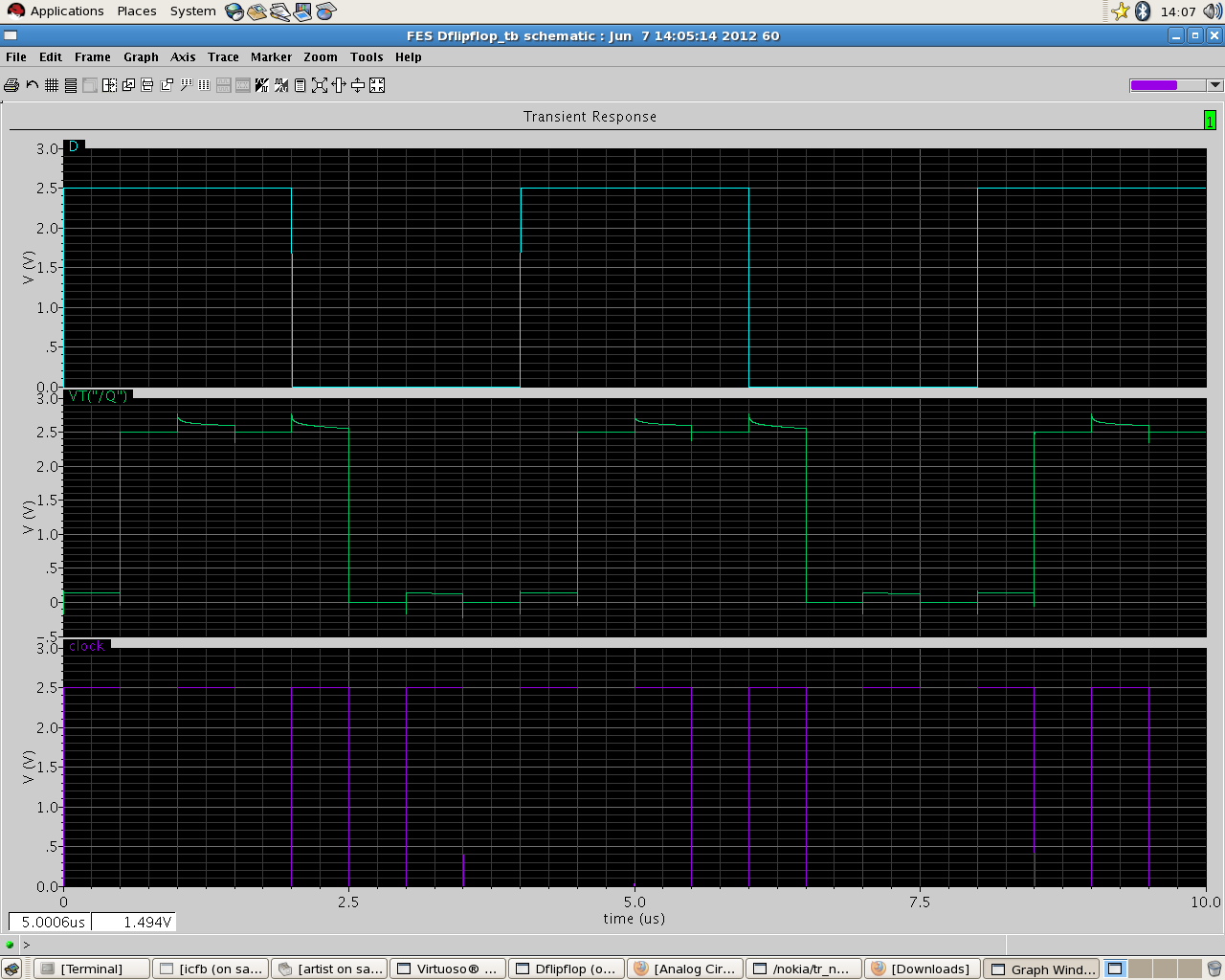
I am simulating Transmission gate D flip flop in cadence but my simulation results show glitches at output. I am attaching my circuit diagram below. Can somebody suggest what is the problem

simulation: Transient
step size 0.1ns
Max step 0.1ns

Input frequency 250kHz
clock frequency 1MHz


- - - Updated - - -

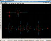
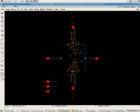
I am also attaching my transmission gate circuit
 

Can you show me the simulation of the signals CLOCK_POS and CLOCK NEG

You get the problem on CLOCK edge ... therefore I think there might be something with your non-overlapping clock generator ....
 
Here are the simulation results for the clock. One picture is zoomed version of other


Is a delay needed between 1st and 2nd transmission gate clocks?
 

You can't drive a T-gate with such an arrangement for clock generation...The way you got it, you are loading the CLOCK_POS more than CLOCK_NEG since it is extra loaded with the inverter producing CLOCK_NEG itself ...

you have to use a non-overlapping clock generation circuit like this one

https://tams-www.informatik.uni-ham.../12-gatedelay/40-tpcg/two-phase-clock-gen.gif

- - - Updated - - -

then use phi1 and phi2 as control inputs to your T-GATE
 
I see two transmission gates, but no FF. To turn the circuit into a D-FF, you need to add some feedback and more transmission gates, I guess.

Two buffers and 4 TGs make a D-FF.
 
Last edited:
Thanks AmrZohny, I made the D-flip flop according to the schematic in the link you provided and it is working now. I am not sure why the previous arrangement was not working because that arrangement is proposed in one IEEE papers.

Amir Ghaffari, Eric, A.M. Kulmperink, "Tunable High Q N-path bandpass filters: modeling and verification" IEEE solid state circuits may 2011 (figure 18).


About your comment on non-overlapping clock generation, i am not able to get the idea. I understand that clock_positive should be equally loaded as clock_negative but what do you mean by overlapping clock generation. Is this overlapping word means that we have to give some delay between clock positive and clock negative?
 

Yes, that's exactly the circuit I mean.

Non-overlapping clock would be preferred, but isn't necessarily required for digital circuits. Standard CMOS logic devices and usual ASIC libraries don't have it. As long as the input doesn't change during clock edge, there's no advantage of break-before-make action.
 

I recommended it since I do not know how big a load viperpaki007 is driving....its advantage is the ability to cascade tapered inverters to be able to drive big loads at the end ...
 

Can you guys suggest some good book regarding basics of CMOS gate circuit design. I am just starting to develop my knowledge in this field and i think i need to understand the basics first.
 

Status
Not open for further replies.

Part and Inventory Search

Welcome to EDABoard.com

Sponsor

Back
Top