Continue to Site

Welcome to EDAboard.com

Welcome to our site! EDAboard.com is an international Electronics Discussion Forum focused on EDA software, circuits, schematics, books, theory, papers, asic, pld, 8051, DSP, Network, RF, Analog Design, PCB, Service Manuals... and a whole lot more! To participate you need to register. Registration is free. Click here to register now.

Help on P Channel Power MOSFET

Status
Not open for further replies.

rosmawati

Member level 1
Joined
Jan 5, 2009
Messages
34
Helped
2
Reputation
4
Reaction score
1
Trophy points
1,288
Location
Penang, Malaysia
Activity points
1,542
Hi,

I would like to confirm my circuit design.
What I planned to do is some kind of switching circuit. It's just that I got confused between drain and source pin of the MOSFET. I've been doing some reading on the net but so far I'm still lost. Did I really hook the connections correctly?
Need your help guys.
Thanks in advance. PMOSFET.JPG
 

Maybe this helps you: Source = E, gate = B, Drain = C for an equivalent PNP transistor. When in on condition, current should flow from source to drain.

Make sure you verify that the mosfet can handle current transients that occur just after on-switching (charging of capacitors).
 

Is that mean my circuit wrongly connected?
Yeah, I got what u meant. Current flows from E to C in PNP transistor. Does that also apply to MOSFET?
 

Yes, this applies to P chan mosfet also (so it will conduct from S to D when the gate is below the source).

Regarding your circuit, I don't understand it well. I hope you can figure it out yourself with the PNP BJT equivalent.

Generally spoken, the power supply is connected to the source and the load to the drain (for a P-channel mosfet).
 

Is that mean my circuit wrongly connected?
the connection is correct. Bulk should have connected higher potential, here supply(its already connected). drain and source can mutually replace the role.
 

Hi,
What I am trying to do is the voltage from Vbatt will OFF when MOSFET gate pin senses VADAPTER. It's more like electronic switching where when VADAPTER goes LOW, voltage from VBAT will flow.
drain and source can mutually replace the role.
Does it also apply to MOSFET? Can it be interchangeable between drain and source?

VADAPTER is 5V while VBAT is 4.2V. The minimum input of the LDO is as low as 3.6V:)
 
Last edited:

drain and source can mutually replace the role.
Does it also apply to MOSFET?Can it be interchangeable between drain and source?
Yes.
Your circuit should work as you intended.Vbat and Vsup will be connected from MOSFET ON.
 

You tell us? I guess it should have been inverted.
But, one question, do you connect separate external diode across MOSFET? Generally, it comes with fabrication. you need not to worry..
 

rosmawati: The body diode is OK.

When +vadapter is open (so no adapter connected), and the switch is closed (battery present), the diode will provide sufficient voltage at +vsup so that the mosfet will conduct and hence the battery current is taken over by the mosfet. This is a good way to eliminate the diode drop.

When you connect the adapter at +Vadapter, Vgs will be zero, hence the mosfet goes off. the body diode prevents charging of the batteries via the adapter.

If this is for a mass production product make sure you add components for ESD protection and other EMC related issues.
 

WimRFP,

It's not mean for any mass production..But I did add a TVS suppressor before +VADAPTER diode for over voltage protection since the main source of +VADAPTER is from wall adapter.
I'll have to wait until the components arrive before I could actually test the circuit. So far, I can only check theoretically. :-D
 

drain and source can mutually replace the role.
Does it also apply to MOSFET?Can it be interchangeable between drain and source?
Yes.
Your circuit should work as you intended.Vbat and Vsup will be connected from MOSFET ON.
Hi Rosmawati, sorry, my statement for your MOSFET IC is not correct.
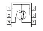
To use PMOS, as switch, source and bulk need to be connected to higher potential. Bulk diode should be reversed for normal operation.
So, connect
Pin 1,2,5,6 = DRAIN to Vbat
Pin 3 = GATE
Pin 4 = SOURCE to +Vsup
 

PMOSFET_body.JPGHi Varunkant2k,
HTML:
So, connect 
Pin 1,2,5,6 = DRAIN to Vbat
Pin 3 = GATE
Pin 4 = SOURCE to +Vsup

That's what i did, right? :???:
 
Last edited:

Sory it should be
Pin 1,2,5,6 = DRAIN to +Vsup
Pin 3 = GATE
Pin 4 = SOURCE to Vbat ( higher voltage)
 

Hi varunkant2k,

I cant test the circuit yet so far. But just wondering what happened when I connect like in the schematic I attached before? Is the MOSFET will going to be broke?
 

Oh yeah? Means when the gate pin HIGH, the PFET is ON?

But I have one example that shows that the input is connected to drain pin. Can you explain a bit on these?
pmosfet_connection_example.JPG
 
Last edited:

But I have one example that shows that the input is connected to drain pin. Can you explain a bit on these?
View attachment 71957
Current diagram has problem of leakage in the bulk, if led-acid battery has lower potential than Vin node. In theory if I talk the current circuit diagram is not correct ( in another word lossy one). The application shown for solar panel is bit complex and has various factor related to real application. In the summer when battery is over charged, need various protectionary measurement. Also the amount of leakage does not affect us, because power source ( for sun) is infinite.
Thats why the circuit diagram is not unacceptable. But still need to do study about the issues related to solar panel charging.( many research already going on).
I am discussing about limited sources application, where you use your circuit in the potable application from battery source.You are worried about power dissipation and other heat sinking/safety problems.
 

Status
Not open for further replies.

Part and Inventory Search

Welcome to EDABoard.com

Sponsor

Back
Top