Continue to Site

Welcome to EDAboard.com

Welcome to our site! EDAboard.com is an international Electronics Discussion Forum focused on EDA software, circuits, schematics, books, theory, papers, asic, pld, 8051, DSP, Network, RF, Analog Design, PCB, Service Manuals... and a whole lot more! To participate you need to register. Registration is free. Click here to register now.

Use of PISCES POSTMINI TOOL

Status
Not open for further replies.

dsrinivasrao

Member level 1
Joined
Oct 9, 2011
Messages
39
Helped
0
Reputation
0
Reaction score
0
Trophy points
1,286
Activity points
1,652
hi all,

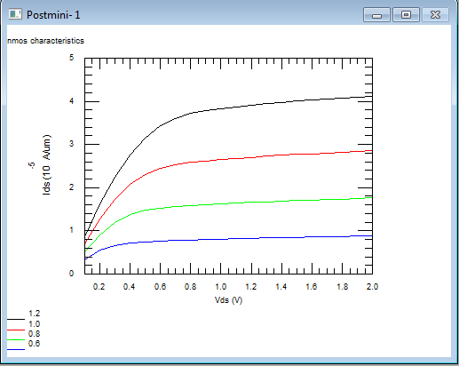
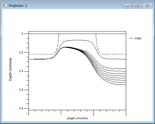
I am Using PISCES POSTMINI TOOL for the device simulation ,Can somebody plz tell me how to plot different curves for same or different variable on the same plot???...Plz help me...
 

Select Overlay in the main menu
->Add (add a plot)
->Delete (delete a plot)
->List (list all plots you are going to plot on same graph)
->Plot (Plot the graphs)
->Exit (return to Post mini main menu)
 

    V

    Points: 2
    Helpful Answer Positive Rating
Thanks a lot..Your suggestions are very helpful i got different potential plots on the same graph..these potential plots are based on the different X-position values..But i want to see different potential plots depending on different gate voltages on the same graph..Kindly help me in this context also..Waiting for ur reply
 

Do you mean 2D contour plots overlaid or overlay of X-Y graph like an Id vs Vd at various Vgs?
 

Yes,I want to see both the things
(1)On the same X-Y graph like an Id vs Vd at various Vgs,similarly for Id vs Vg at various Vds,also
(2)I want to see potential(as a variable) graph along my grid at various Vg and Vd applied...Like,as soon as i increase my Vd from 1v to 5v through a step of 1v,my drain-body junction becomes more and more reverse biased hence I have to see potential increase in steps in the same graph..

Hoping that this tym i am clear with my doubt...
 

For example of the Id vs Vd vs Vg, I would run each Vd ramp (at Vg) and log it to its own file. So there would be a IdVd file for each Vg. These would be something like
idvd0P2.log results of sweeping Vd for a Vgs=0.2V
idvd0P4.log results of sweeping Vd for a Vgs=0.4V
...etc.
Now assume the terminals in Pisces are 1=D 2=G 3=S 4=Sub
In Postmini

Overlay->Read->Ascii->idvd0p2.log

This brings up the Read Ascii Data File window. Need to skip line 1 of the log file which is just the number of terminals. So

6->1

The X axis data for Vds (terminal 1) are in column 2 of a log file.

2->2

The y axis data for Ids (terminal 1) are in column 10.

3->10

All other defaults are OK so just accept this

ACCEPT

Now add this curve to the list to be plotted and label it

ADD

1->Label for curve

ACCEPT

Now plot it and add graph title (this is first plot with only one curve)

PLOT

1->Title for graph

PLOT

You should now have the graph with 1 curve on it. You can now add X,Y axis labels etc.

9->Vds
10->V
18->Ids
19->A/um

PLOT

Ok now to add more curves

EXIT

READ (accept defaults) enter filename.log

Since defaults should be ok just accept this

ACCEPT

ADD

1->curve label

ACCEPT

PLOT

PLOT

You should now have 2 curves, so just repeat this until you get bored stiff or run out of curves.

Cover other plots in next reply

 
Next .........

Using the previous example, lets set Vg = 1.2V and ramp Vd from 0 to 2.0V
I have saved a solution file for each Vd is steps on 0.2V from 0 to 2.0V
We will now display the progression of zero potential contour with Vd.

In Postmini main menu:

COMPARE

This gives the comparison contour plot

READ ->PISCES->whatever.msh ->Soln0.slv
ADD
What to see potential contour so select potential

2

Plot attributes for entry - use contour for zero potential

17-> 0.0

ACCEPT ->EXIT

PLOT
PLOT
Can now see the 1st contour plot which is coloured will filled contours

READ ->PISCES->whatever.msh ->Soln1.slv
ADD ->2 ->17 ->0 ->ACCEPT ->Exit
READ ->PISCES->whatever.msh ->Soln2.slv
ADD ->2 ->17 ->0 ->ACCEPT ->Exit
etc
etc

PLOT
PLOT

Can now see all plots - but you cant because being shaded, they over write each other

so need to turn off contour fill.

EXIT to get back to Comparison Contour plot menu.

MODIFY
Select 1st contour plot and turn off contour colours...
1 -> 2 ->EXIT
2 -> 2 ->EXIT
etc

Now the plot has the contour for the zero potential as a function of Vds.


Hope this has helped!


---------- Post added at 16:58 ---------- Previous post was at 16:41 ----------

Spot the deliberate (huh) mistake, I go OVERLAY and COMPARE round the wrong way!!
 
  • Like
Reactions: dsrinivasrao

    V

    Points: 2
    Helpful Answer Positive Rating

    dsrinivasrao

    Points: 2
    Helpful Answer Positive Rating
hello colbhaidh...I got rid of my all problems..thankkkkkkkkkkkkkksssssssssssssssssss a lottttttttttttttttttttttttt buddy.....U are just simply awesome man.......i am very happy..........Kindly accept my friend request...U know u actually solved my 50 percent problems which i am facing in my Masters Thesis..dats so nice of u ...

Now i have to see charge injection at drain side at different gate voltage fall times??..I had created a holding capacitor on the drain side..So can u please guide me how to proceed,if possible then only......
 

Set up drain contact with a resistance and capacitance, then solve the transient on the gate from gate on to gate off:

CONTACT NUM=<drain> RESIS=<??> CAP=<??>
SOLVE V<gate>=3.3 RAMPTIME=<??> DT=<??> TSTOP=<??>

Remember the capacitance is F/um and resistance is Ohms.um.
Look at channel charge contours as the deviuce is turning off to see where charge is dispersing.

Remember that in reality, the gate will not ramp off linearly. There will be some oscillation of the Vgate increasing in magnitude prior to the rapid drop towards zero. Then there will be a minimum below zero before recovery to zero volts.
These ringing effects will impact the charge dispersal. But worry about that later, just get the simple stuff working first.
 
hi,
I am trying the steps u told for my grid..but when i am putting resistance in my drain contact a error is coming like,Full newton required with the dumped elements,
contact resistance or current BC 252..I am attaching photos of my current Pisces grid and transient file..kindly check it.

45_1330187875.jpg


But when i putting "contact resistance" in place of "resistance",

eg:- contact 4 (for drain) neutral con.res.....this is working properly???

plz solve this....Also throw some light on convergence issue in pisces....
 

Since this is 0.18um 4nm gate oxide, the maximum voltage on the gate should not exceed 5MV/cm so use 1.8V as the gate voltage. Try the following:


TITLE ... MOSFET 180nm transient on gate

mesh infile=7grid2
contact num=1 n.poly
contact num=2 neutral
contact num=3 neutral
contact num=4 neutral cap=0.5E12 res=1.0e3

symb newton carriers=1 electrons
method 2nd Tauto autonr
solve init currents
log outf=ivtran.log
solve v4=0 v1=0 v2=0 v3=0
solve v1=1.8 ramptime=5e-9 dt=1E-9 tstop=20e-9 currents outf=a0
solve v1=0.0 ramptime=5e-9 dt=1E-9 tstop=20e-9 currents outf=b0
end

Just change the times to suit your experiments. Check your LDD regions (doping at edge of gate) they do not look right.
 

    V

    Points: 2
    Helpful Answer Positive Rating
Hi Colbhaidh thnx for your valuable tips and support..I have some questions regarding my grid..

1)Is it necessary to use gate terminal as n.ploy or can i use neutral??
2)You asked me to check the grid again..are u saying about doping card of the grid & what does LDD regions mean??
3)In making my rectangular grid i defined my y.mesh has n=1 to n=5 in oxide layer and from n=6 onwards is present in silicon..
But in the region card i defined oxide region from n=1 to n=5..Is it correct?? Shouldn't it be from n=1 to n=6?? i had connected the source and drain terminal from n=6??.
4)If i put a source resistance Rs=10K and allow gate voltage to from ON to OFF,i should see that the channel charge should move towards drain since there is resis on source side..So to look after this channel charge which contour lines i should look??Whether i should see electron concentration contour or any other specific contour??

thanx a lot...
 

(1) You need the gate to be n.poly or p.poly to make sure the threshold voltage will be correct as this defines the barrier potential or workfunction of the poly gate. This makes sure the surface charge during simulation is correct. For 0.18 then nmos will always have n.poly and pmos p.poly.

(2) The LDD is the doping from the source drain that is beneath the gate poly. It is usually lighter doped than the SD junctions. For 0.18um, the doiping would reach at least 0.1um beneath the gate on each side. This doping creates the miller capacitance between the gate edges and the SD implants and can contribute significantly to charge injection. Typically at 0.18um physical gate length produces a 0.15-0.16um actual length (Effective Length). Moving the gaussian doping edges closer to the gate should fix this.

81_1330337782.png


(3) Since y node = 6 is the start of the silicon, I think you are correct as it stands. If not, it would not work as the source and drain contacts would be in oxide and therefore not conduct. Leave as is.

(4) Look at charge contours and how they move. I think you need to have a capacitance on the drain though.
 
Hi colbhaidh.....Thank you very much for your support..As you said I need to have a capacitance on drain side to see charge injection,same was told by my prof..So i prepared the Holding capacitor on the drain side..What i did was,as i need to have two metal plates and a oxide layer to form the capacitor, i used my n+ region of drain side as my upper plate of capacitor and the oxide layer of 1nm (which is already there in grid) and put a metal (electrode=4) on it as bottom plate of the capacitor.so this will form my capacitor,so now i have to ground bottom plate(which is electrode=4)of cap while doing a transient and dc analysis..

Holding Capacitor=Ch
Gate Capacitor=Cg
Esi=E=3.9*8.854E-12
w=width of device=1um
Tox,h=oxide of holding cap=1nm
Tox,m=oxide of mosfet=4nm
Lg=gate length
Lh=Holding capacitor length

Ch/Cg = ((E*Lh*w)/Tox,h)*(Tox,m/(E*Lg*w))

= 4*(Lh/Lg)

so i can adjust the length of my Lh to get the required Ch value..Here i make it Ch=16Cg..As my gate length is .18um i made my drain region as 0.72um..i am attaching my grid..

But when i am doing the dc analysis,it is not converging for higher values of source voltages..also when i am putting the carrier=2 it is converging for higher values of source voltages then previous one????..Can u have a look at it and it will be so kind of u if u can correct it or give me the reason what can be the issue??..

15_1330384974.jpg
 

hi.....I created the capacitor on the drain side....I run the transient analysis with different fall times and had saved the different solution files..
But when i am seeing electron concentration contour lines by the Overlay method i am not able to see any graphs..Am I doing correct method or not?? I have to look after electron concentration or the net charge contour??

Do i have to use Compare method instead of overlay so that i can see the charge injection??

Pleeeezzzzzz clarify my doubts....

Thank you in advance..
 

change
contact num=4 neutral
to
contact num=4 alum

When tou specifiy neutral, Pisces calculates the work function from the mesh. You have oxide here so neutral will cause the capacitor to fail as there is no conductor.
 

    V

    Points: 2
    Helpful Answer Positive Rating
hi...thanx a lot friend...the way you explain pisces II commands is wonderful...Thanks a very much..Now i have a good hold over DC and Transient analysis,its because of u only..

Actually now i want to find gate capacitance Cg of my previous grid (the one without holding capacitor)..For this i have to do an AC analysis..so my set up will be like the one shown in the image..In this source,drain and body terminal will be grounded and an Voltage V1(ac+dc) should be applied to the gate..


I had written the code::

title AC analysis
$
mesh infile=7grid2
contac num=1 n.poly (gate)
contac num=2 neutral (bulk)
contac num=3 neutral (source)
contac num=4 neutral (drain)

symb newton carriers=2 electrons
method 2nd Tauto autonr
solve init currents
log outf=ac.log
solve v1=0.2 v2=0 v3=0 v4=0 currents
solve AC.analy freq=1E4 fstep=10 nfsteps=100 vss=1 terminal=1 currents outf=ac
end

but some error is coming..Even though i specified terminal=1 in the ac.log file,the first line has number 4 in it,which means it is solving for drain terminal instead of gate terminal..also it has just two solution in the log file..Can u please correct,i tried whole day running the code but end up with no result..Plz help me...

What to do if we want to find gate current at each frequency??..
So if i increase dc voltage on my gate terminal,my transistor will move from cut off to linear and then to saturation region and each time Cg will change according to region of working.So i will be able to plot C-V plot of my transistor..Am I approaching the right method??? Kindly help me...
 

The 4 means there are 4 terminals in the log file, so this is correct.
The following rows are arranged in columns
Not_sure, T1 (V), T2 (V), T3 (V), T4 (V), T1 (V), T2 (V), T3 (V), T4 (V),T1 (soln),T2 (soln),T3 (soln),T4 (soln)

each row is the solution at each point of the simulation. The last 4 columns are the ones with the relevant solution (currents etc)
 

I forgot to add...
When running Pisces in windows, yopu would normally enter the command line

pisces2 myinput.p2

then psices would output a whole lot of stuff in the coomand prompt window which will be lost by the end of the simulation.
To capture this stuff, enter the command as follows:

pisces2 myinput.p2 > tmp.txt

Nothing will appear in the command window but everything will be captured in the file tmp.txt which you can view with any text editor. For the capacitance measurements, the actual capacitances are not put in the outf=ac file but will apprear in the command window. If you capture everything to tmp.txt you will have all the results.
The last output to the windows will have been :

Ac analysis :
Ac voltage = 1.000000E+00
Frequency = 1.100000E+04 Hz


Electrode # 1

Electrode Conduction Current Displacement Current
(amps/micron) (amps/micron)
1 0.00000E+00 0.00000E+00 3.42495E-19 8.73996E-11
2 -4.74229E-19 -6.76463E-12 1.52460E-20 -1.45151E-18
3 5.78599E-17 -4.32588E-11 5.12848E-21 -4.57651E-13
4 1.38796E-16 -3.64566E-11 4.30420E-21 -4.61906E-13


Element Total Current Conductance Capacitance
(amps/micron) (siemens/micron) (farads/micron)
Y11 3.42495E-19 8.73996E-11 3.42495E-19 1.26455E-15
Y21 -4.58983E-19 -6.76463E-12 -4.58983E-19 -9.78749E-17
Y31 5.78650E-17 -4.37165E-11 5.78650E-17 -6.32517E-16
Y41 1.38800E-16 -3.69185E-11 1.38800E-16 -5.34160E-16

Absolute convergence criterion met for Poisson
Absolute convergence criterion met for continuity
Total cpu time for bias point = 0.59
Total cpu time = 0.89
Solution written to ac

---------- Post added at 21:50 ---------- Previous post was at 21:01 ----------

To get the classic CV plot (sweep -Vg to +Vg), use the following:

TITLE ... MOSFET 180nm CV
mesh infile=7grid2
contact num=1 n.poly
contact num=2 neutral
contact num=3 neutral
contact num=4 neutral
symb newton carriers=2 electrons
method 2nd Tauto autonr
solve init currents
log outf=ac.log
solve v1=0 v2=0 v3=0 v4=0
solve AC.**** freq=1.0E6 elect=1 vstep=-0.2 nsteps=9 VSS=0.01 outf=ac1
solve v1=0 v2=0 v3=0 v4=0
solve AC.**** freq=1.0E6 elect=1 vstep=0.2 nsteps=9 VSS=0.01 outf=ac2
end

run pisces2 0p18CV.p2 > tmp.txt

From tmp.txt extract the capacitances for electrode 1 into excel or something and plot vs Vg.

 
Thank you very much....U have the best Pisces Knowledge among the people I contact...thnx a lot for ur help...
I have some some doubts regarding Clock feedthrough..

Whenever our transistor gets off two effects take place which creates error at the output (1) Our channel charge (Qch=W*L*Cox*(Vgs-Vth)) will flow to source and Drain,hence creates the error,this error depends upon the fall time of gate voltage also (2)
the overlap cap and the holding Cap form a potential divider circuit and hence also causes the error.

Error Voltage Vo=(Cov/(Cov+Ch))Vin..

So how to see it in pisces???...

One way which i think is to give 0.3v dc + 10mv ac on the gate terminal,as dc voltage < vth(0.4),transistor is always off and the error in output will be because of only
colck feed through,hence if I plot potential plot and find the voltage at output (i.e,drain terminal),if there is diff between source and Drain terminal voltage then that vil be
because of clock feed through only..So what i am thinking is correct or not???

Also in postmini one option is there "Window",i selected it and then selected the 'style' of windows,from that i selected the multiple window but the present plot(window wich containgraph of potential etc)window gets disappeared..So what is happening i dont know about it anything...Plz help me in this context also...Pleez i waiting for ur reply...
also get disappeared

Plz help me......
 

Status
Not open for further replies.

Part and Inventory Search

Welcome to EDABoard.com

Sponsor

Back
Top