Continue to Site

Welcome to EDAboard.com

Welcome to our site! EDAboard.com is an international Electronics Discussion Forum focused on EDA software, circuits, schematics, books, theory, papers, asic, pld, 8051, DSP, Network, RF, Analog Design, PCB, Service Manuals... and a whole lot more! To participate you need to register. Registration is free. Click here to register now.

Mos current mode logic

Status
Not open for further replies.

Neetha Patil

Junior Member level 2
Joined
Jan 9, 2012
Messages
23
Helped
0
Reputation
0
Reaction score
0
Trophy points
1,281
Location
India
Activity points
1,465
Hiiiii
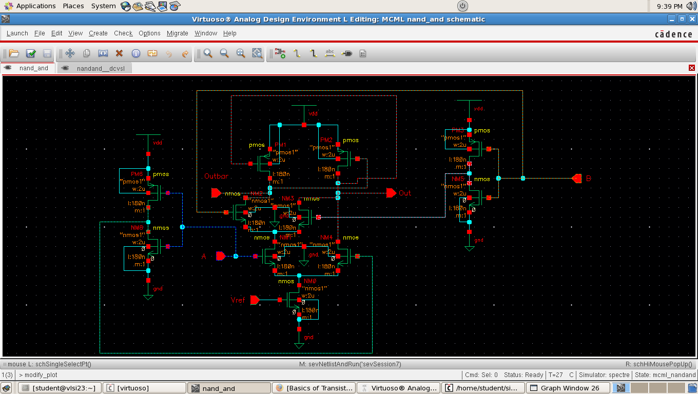
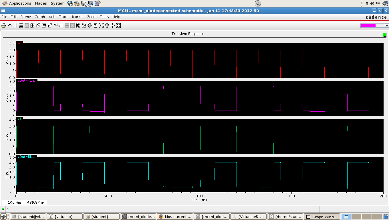
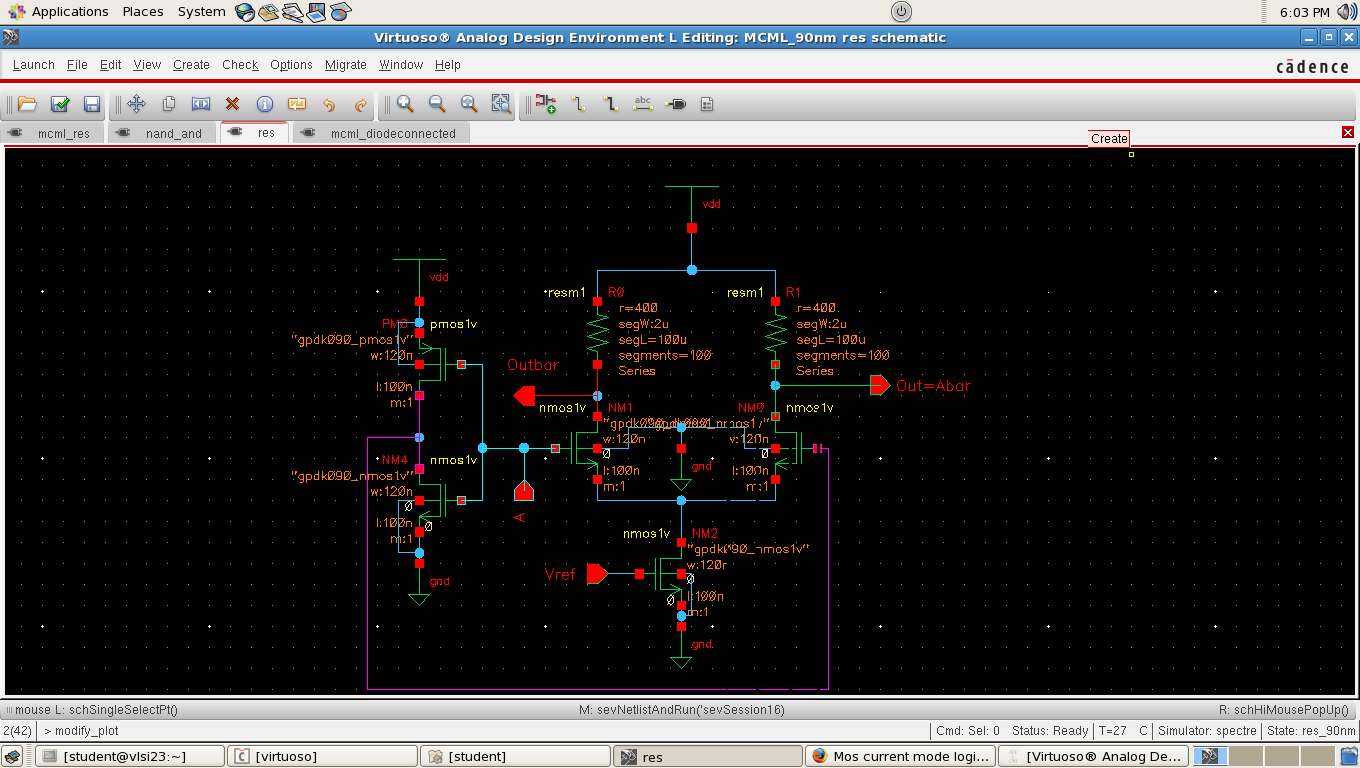
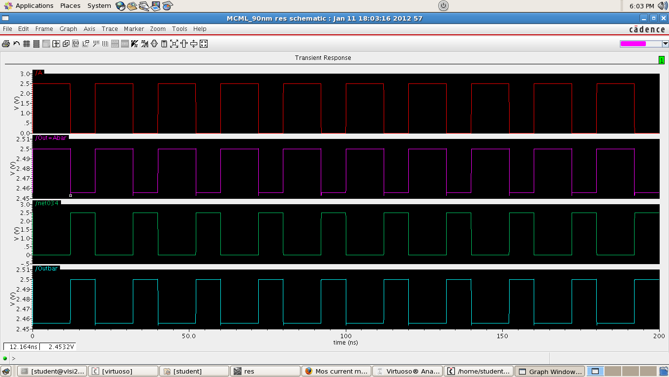
I am doing my thesis on Theoretical Analysis of Mos current mode logic(MCML) by using Cadence(Tool) Virtuoso . I am getting problem during simulation while placing Nand/And logic in place of Inverter Logic and kept Pmos in triode region(Gate to drain is shorted). The output and OutBar should be get and/Nand but iam getting And/Or please help me to solve problem.

Thank You
Regards
Neetha

---------- Post added at 01:31 ---------- Previous post was at 00:52 ----------
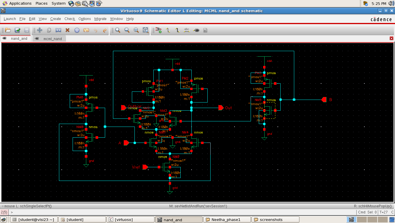
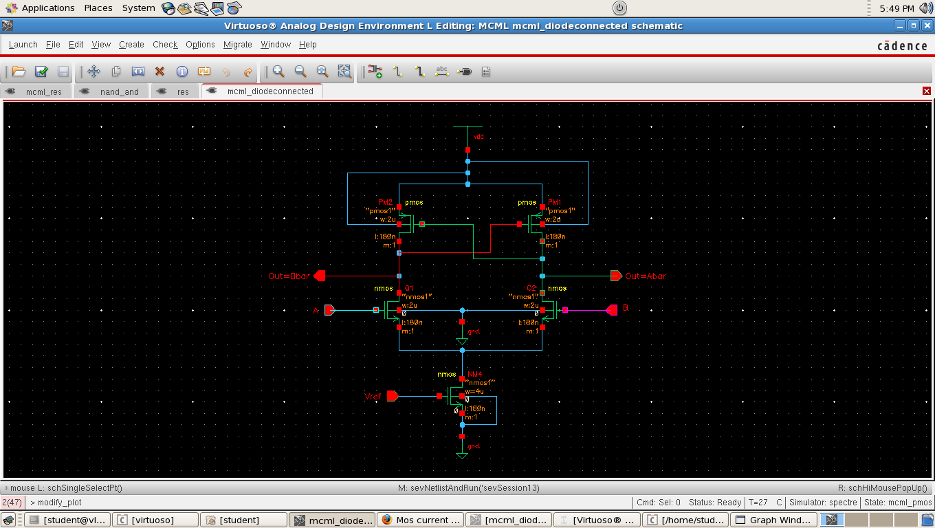
 

Question is not clear. In CML, the structure for OR,AND,NOR and NAND are same. Only the way in which the inputs and complementary inputs are connected and the way output is taken, decides the function. The PMOS diodes PM1 and PM2 should be much weaker than rest of the devices


This is the my schematic, as u said the structure is same but iam getting outputs are and/Or functionality instead of and/Nand

---------- Post added at 15:10 ---------- Previous post was at 15:01 ----------

as my inputs/outputs are A,B,Out for AND logic and Abar,Bbar ,Outbar for NAND logic while simulating in virtuoso iam getting o/p's are AND/Or functionality where is the error iam unable to find and for the load Pmos to be operated in the linear / Triode region i shorted GAte and drain. Is it Correct and please give the solution to find out error.

Thank U
 

If your inputs/outputs are A,B and Out for AND logic, the inputs/outputs should be A,B and Outbar for NAND logic. If you complement everything in a AND gate you should get OR function which is exactly what you are seeing.
When you short the gate and drain of a MOS, it can only operate in saturation or in cutoff, not in triode.
 
Thank You sir :) .that means for A,B inputs we have to check out and outBar not for Abar,Bbar .


as u said i connect pmos like that only i got the output . but to operate in triode region why should it connect like that only is anything reason behind it if yes please explain it


Thank You in Advance:)

---------- Post added at 23:08 ---------- Previous post was at 22:27 ----------

one more doubt plz for transistor nmos7 to operate in saturation region how much Vref should give in my thesis iam giving 0.8 v and 1v .and vdd giving 2.5 v in 180nm tech.my doubt is for gpdk 180nm and gpdk 90nm tech how much should dive vdd and Vref please explain me
 

You should no first why Triode region required ?: For linearly controlling the change in input your output voltage should vary accordingly. That means, your voltage drop across load transistor should linearly vary with input voltage to adjust the output voltage Common mode.
If you operate your load transistor in saturation, it may not be controlled linearly with input voltage variation.
nmos7 to operate in saturation region how much Vref should give in my thesis i am giving 0.8 v and 1v .and vdd giving 2.5 v in 180nm tech.
I did not get "NMOS7" but NMOS to operate in saturation its Vds should always be greater than Vgs-Vth. where Vgs >/=Vth.

---------- Post added at 12:08 ---------- Previous post was at 12:06 ----------

Linear region is required because its output closely follows the rail voltage ( VDD)
 

Thank You sir :).for gpdk 180nm and gpdk 90nm technology how much vdd should give .In my thesis iam giving 2.5v vdd I think we can give upto 5v .what is the specification of vdd how it useful to design.if minimum gives what happend and if maxum?

Nmos7 means this the last transistor below pull down network in my schematic which has Vref as a input which i given 0.8v / 1v (>vth) to operate in saturation .as u said to operate in saturation Vds>= Vgs-Vth how it related means my input is Vref fixed voltage .in this also how much Vref should give it should be (>Vth = 0.7) that i know how much maMinximium can give ? Is it depends on Vdd= 2.5V.My question is Vref is related to VDD? if yes how it is and how much should give Vref and Vdd Min and Max in gpdk 180nm and gpdk 90nm technology.
Here is my schematic:


---------- Post added at 17:10 ---------- Previous post was at 17:05 ----------

How Current will calculate in Virtuoso? iam clicking at the drain nodes at the output for current calculation is it right?this is the result of nand/and logic in MCML
 

Check your PDk and confirm if devices can support 5Volts.There are very basic difference in 2.5V and 5V operation.
Low Volts: low power consumption, and smaller device sizes
High volts: High power consumption, bigger device sizes
Again high speed are achieved at low voltage signalling.
how much Vref should give it should be (>Vth = 0.7) that i know how much maMinximium can give ?
You give Vref =VDD and check if lower transistor is still in saturation. If you give Vref VDD, NMOS7 will go in triode region.and will not work as current sink. There is range for Vref from Vth+0.7 to Vth+(Vdd- Voltage Drop across PM1,NM1 and NM2).

How Current will calculate in Virtuoso? iam clicking at the drain nodes at the output for current calculation is it right?
Yes that is correct
 

You give Vref =VDD and check if lower transistor is still in saturation. If you give Vref VDD, NMOS7 will go in triode region.and will not work as current sink.
.

I didnt get u sir , i give Vref= 1.2 v[ which is >Vth=0.7 and <VDD=2.5v].in wave forms/Design how can know whether it is woking in saturation or in triode region.Lower transistor means in my schematic is it NMOS5 which has i/p Vref?

There is range for Vref from Vth+0.7 to Vth+(Vdd- Voltage Drop across PM1,NM1 and NM2).

I didnt get u the above statement, already Vth=0.7 and again have to add 0.7? Vth+(Vdd- Voltage Drop across PM1,NM1 and NM2) =?
this my schematic and waveform for nand/and logic in MCML iam getting correct result or not i mean nmos5 is in saturation / triode ?


Thank u in advance
 
Last edited:

There is range for Vref from Vth+0.7 to Vth+(Vdd- Voltage Drop across PM1,NM1 and NM2).
already Vth=0.7 and again have to add 0.7?
Sorry, I mistakenly written Vth +0.7. instead Vth+drop across NMOS5 = Vth + 0.3V

---------- Post added at 15:50 ---------- Previous post was at 15:47 ----------

didnt get u sir , i give Vref= 1.2 v[ which is >Vth=0.7 and <VDD=2.5v].in wave forms/Design how can know whether it is woking in saturation or in triode region.
I think You have to calculate voltage drop across active path from NMOS5 to VDD. This you can do by using current flowing from each transistor. I already mentioned maximum value of Vref can go upto "Vth+(Vdd- Voltage Drop across PM1,NM1 and NM2)"
 
Check your PDk and confirm if devices can support 5Volts.There are very basic difference in 2.5V and 5V operation.
Low Volts: low power consumption, and smaller device sizes
High volts: High power consumption, bigger device sizes
Again high speed are achieved at low voltage signalling.

i AM USING GPDK 180NM TECHNOLOGY AND GIVEN VDD=2.5 V .IS IT GOOD DESIGN WORKING WITH LOW vdd .I MEAN WHICH SHOULD PREFER WHETHER 2.5V OR 5 V AS A VDD
 

Most of older book references are given in 3.3V/5V so better go for 5V.Other than if you don't have specific purpose, I may not tell which voltage should be preferred.
 
Hiiiiiiii sir
i added gpdk 90nm tech library in the sys in which i worked in gpdk 180 nm tech, if we added like that then it will work or not ?and if i want to do at a time 180nm and 90nm in diif tabs in window it will work or not ? other wise i have to do different systems for diff libraries? because iam not getting results of simple inverter logic in MCML in both 180nm and 90nm tech with load as resitor and load as pmos in both cases . but if i check my nand/and logic its running and gives same result which i got before. i am attaching my schematic please tell me where is error.

this is 180nm tech with resistor as load in MCML and their waveforms .


this is 180nm tech with pmos as load in MCML and their waveforms .


this is 90nm tech with resistor as load in MCML and their waveforms .
 
Last edited:

There is very basic errors:
1. Schematic one ( with resistive load) : why these resistances are this small? Guess, if IN is high, Out1 should be low. For this how much voltage drop do you expect across resistance R2. It will not be low. the same for reverse. Reason is gain is very low. You should have used PMOS latch.
2. Schematic Two ( with PMOS latch): A and B are two different signals. For invertion you should have complementary signals.

and common point: A and B signal should have minimum voltage and maximum voltage levels to use CML logic. If A and B are zero together how you expect that circuit will still work.
 

Sorry sir i didnt get u i gave a =0 to 2.5v and b= 2.5 to 0 vwhich are different for pmos as a load
and resistors small means i didn get ?if u dnt mine plz can u explain in another way
for ex: how much res valua and A,B values then i will check once again

---------- Post added at 18:45 ---------- Previous post was at 18:43 ----------

i added gpdk 90nm tech library in the sys in which i worked in gpdk 180 nm tech, if we added like that then it will work or not ?and if i want to do at a time 180nm and 90nm in diif tabs in window it will work or not ? other wise i have to do different systems for diff libraries?[

What about dis sir?

---------- Post added at 18:49 ---------- Previous post was at 18:45 ----------

Schematic Two ( with PMOS latch): A and B are two different signals. For invertion you should have complementary signals.

yes sir i agree with u thats y i give 0 to 2.5(Logic 1) and Logic 0 for signals i gave the names as A,B for my purpuse

---------- Post added at 18:52 ---------- Previous post was at 18:49 ----------

There is very basic errors:
1. Schematic one ( with resistive load) : why these resistances are this small? Guess, if IN is high, Out1 should be low. For this how much voltage drop do you expect across resistance R2. It will not be low. the same for reverse. Reason is gain is very low.

Resistance small means i didnt get u sir how much Resistance value shoulg give ?
 

If you want to use inverter , why don't you go for simple push-pull inverter? why differential one you want? Simple inverter is faster and consumes less current.
This architecture you use is for working in the linear region. And due to very low gain, it needs another stage for rail to rail amplification.
 

this is 90nm tech with resistor as load in MCML and their waveforms .
If you want to analyze Inverter from NAND and NOR logic's, better use NAND shorted inputs. Differential pair is a bit complex architecture, you need to read the differential pair design thoroughly.

---------- Post added at 10:31 ---------- Previous post was at 10:27 ----------

If you want to use your schematic 1 and 2 to work with your architecture, use latch/inverter in the second stage.
 

Hiiiiii
my basic gate is MCML Inverter from this iam doing Nand/And,Nor/Or Logics. i am getting results of both why cant inverter where is the error . how much use resistance , VDD, Vref for the inverter .{ gain = V0/Vin here in my case both o/p and i/p voltages are equal }. is there any connections error or else values .please tell me sir

Thank u in advance
 

Status
Not open for further replies.

Part and Inventory Search

Welcome to EDABoard.com

Sponsor

Back
Top