The_Dutchman
Member level 1
Hello,
I can't figure out a fool proof way to determine the minimum and maximum output voltage swing of a CMOS circuit. I really don't see it.
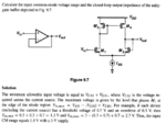
Take this example.

I know that for saturation, |VDS| > |VGS| - TH
So I guess for NMOS it means that the drain voltage can maximum be a treshold under gate voltage.
I think that the VGS has to be at least the treshold voltage + overdrive voltage ?
For the PMOS it is the same but opposite signs.
Is there a fool prove way to find the voltage swings? I've broken my mind many times over it.
From the example, the maximum voltage is VDD-VGS3+VTH1. I guess they are driving the drain voltage of M3 one treshold voltage higher than the gate voltage. But why VTH1 and not VTH3?
I'm trying to determine the minimum and maximum of vout.
I've found so far:
-Minimum: Vout = Vcss + Vgs2
-Maximum: Trying.... (M3 and M4 form current mirror, so VGS4 is fixed) so i think: VDD-VGS4+VTH4
please correct me if I'm wrong
Thanks in advance.
I can't figure out a fool proof way to determine the minimum and maximum output voltage swing of a CMOS circuit. I really don't see it.
Take this example.

I know that for saturation, |VDS| > |VGS| - TH
So I guess for NMOS it means that the drain voltage can maximum be a treshold under gate voltage.
I think that the VGS has to be at least the treshold voltage + overdrive voltage ?
For the PMOS it is the same but opposite signs.
Is there a fool prove way to find the voltage swings? I've broken my mind many times over it.
From the example, the maximum voltage is VDD-VGS3+VTH1. I guess they are driving the drain voltage of M3 one treshold voltage higher than the gate voltage. But why VTH1 and not VTH3?
I'm trying to determine the minimum and maximum of vout.
I've found so far:
-Minimum: Vout = Vcss + Vgs2
-Maximum: Trying.... (M3 and M4 form current mirror, so VGS4 is fixed) so i think: VDD-VGS4+VTH4
please correct me if I'm wrong
Thanks in advance.
Last edited: