Welcome to our site! EDAboard.com is an international Electronics Discussion Forum focused on EDA software, circuits, schematics, books, theory, papers, asic, pld, 8051, DSP, Network, RF, Analog Design, PCB, Service Manuals... and a whole lot more! To participate you need to register. Registration is free. Click here to register now.
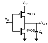
CMOS inverter:
Fig : CMOS Inverter
VIN
Vout
NMOS
Region of operation for NMOS
PMOS
Region of operation for PMOS
< Vtn
VOH
Off
Cut off
On
Linear
VIL
VOH
On
Saturation
On
Linear
Vtn = VDD/2
VDD/2
On
Saturation
On
Saturation
VIH
VOL
On
Linear
On...
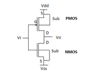
CMOS:
CMOS stands for Complementary Metal Oxide Semiconductor Field Effect Transistor.
nt
Fig: CMOS circuit
Advantages of CMOS:
High noise margin due to full voltage swing.
High input impedance due to IG = 0.
Low output impedance, in steady state there always exists a path with finite...
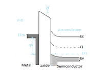
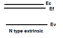
Energy band diagram:
Equilibrium :
In ideal conditions there is no external supply to the device so the energy gap between conduction and valence band is high.
The gap between Evac and Efm is called the work function qΦm is the energy required by an electron to move from Fermi energy to...
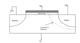
Short channel device:
A device is said to be short channel if it has following properties:
A device is called a short channel if its channel length is <1µm.
If the channel length is in the order of depletion region width at source and drain junction it is a short channel device.
If the...
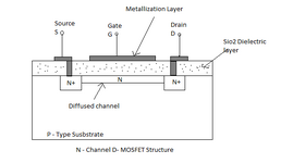
Depletion MOSFET
Depletion N MOSFET:
Fig: NMOSFET - depeletion
VGS = 0 volts VDS > 0
Though the VGS is zero volts but due to external supply at drain and the presence of channel the electric field from drain causes electrons from source to travel from source to drain there by causing...
MOSFET:
MOSFETs are chosen for VLSI applications instead of BJT’s because MOSFETs can handle high frequency operations but BJT can’t so MOSFETs are preferred over BJTs in VLSI circuits.
MOSFET stands for Metal Oxide Semiconductor Field Effect Transistor.
Enhancement N MOSFET :
Zero bias ...
PN junction:
Fig: PN junction open circuit
Fig: PN junction characteristics
Open circuit PN-junction:
Fig: open circuit PN junction
Diffusion current component:
As we have holes as majority in P side and electrons in N side there is concentration gradient on both sides which leads...
Fundamentals of electrons and holes:
Let’s begin our discussion from basics which is about atoms, electrons and their properties. As the MOSFET deals with both electrons and holes we need to have a clear idea on what the internal operation is in a circuit.
Let’s focus on two special points in...
This site uses cookies to help personalise content, tailor your experience and to keep you logged in if you register.
By continuing to use this site, you are consenting to our use of cookies.